

 Material testing and consumables
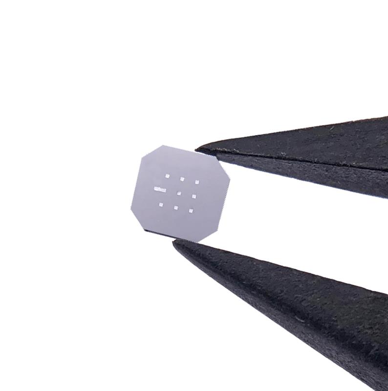
产品:TEM nanoporous silicon nitride film
ID:BK2020040433
CAS:51-18-3
price: Inquiry
Item ID:BK2020040433-01
specification:
Detailed
The TEM silicon nitride film pane produced by Beike Nano is produced by advanced microelectronics technology and can be used for high-resolution electron microscopy observation of micro-nano samples. This pane is an octagon with a 3mm outer diameter and is suitable for all TEM sample rods. To be suitable for a variety of experimental conditions, Beike Nano provides scientific researchers with single pane, multi pane and micropore pane standard product. The silicon nitride film adopts low-stress technology (<250MPa). The silicon nitride film is thin and not easily damaged. It is very suitable for cutting-edge research in biology, materials, physics, and chemistry.
Features
Ultra clean
Class 100 clean environment
Strict selection of silicon substrate materials
Advanced technology level
high strength
Film stress <250Mpa
The thinnest film can reach 10nm
The window size can be up to 2cm
Super smooth
Roughness less than 0.5nm
Uniformity is better than 5%
Excellent physical and chemical stability
Acid resistance (except hydrofluoric acid), alkali resistance, organic solvent resistance
Easy to use plasma cleaning
High current electron beam tolerance


Technical Parameters
| Outer frame items | parameter | Outer frame items | parameter |
| material | N -type silicon | Resistivity | 1 ~ 10 Ω-cm |
| Silicon nitride film parameters | parameter | Silicon nitride film parameters | parameter |
| material | LPCVD silicon nitride film | stress | <250MPa |
| Dielectric constant | 6-7 | Dielectric strength | 10 (10 6 V / cm) |
| Resistivity | 10 16 Ω-cm | Roughness (Ra) | 0.28 ± 5% nm |
| Young‘s modulus | 270GPa | Roughness (Rms) | 0.40 ± 5% nm |
Application range

Nano materials, semiconductor materials, optical crystal materials, functional thin film materials

Characterization experiments of colloids, aerogels, organic materials and nanoparticles

Analysis of carbon-containing samples (photoresist, polymer, food, oil, fuel, etc.)

As a biological and cellular carrier
Product specification
- the TEM single-pane silicon nitride film -
Substrate 200um thick, 3mm diameter standard TEM silicon nitride window
| Product ID | Film thickness | Window size | Buy now |
| SG010Z | 10nm | 0.10 × 0.10mm |
|
| SG015Z | 10nm | 0.15 × 0.15mm |
|
| SG025Z | 10nm | 0.25 × 0.25mm |
|
| SG050Z | 10nm | 0.50 × 0.50mm |
|
| SG025A | 15nm | 0.25x0.25mm |
|
| SG050A | 15nm | 0.5x0.5mm |
|
| SG100A | 15nm | 1x1mm |
|
| SG025B | 30nm | 0.25x0.25mm |
|
| SG050B | 30nm | 0.5x0.5mm |
|
| SG100B | 30nm | 1x1mm |
|
| SG025C | 50nm | 0.25x0.25mm |
|
| SG050C | 50nm | 0.5x0.5mm |
|
| SG100C | 50nm | 1x1mm |
|
| SG050D | 100nm | 0.5x0.5mm |
|
| SG025E | 200nm | 0.25x0.25mm |
|
| SG050E | 200nm | 0.5x0.5mm |
|
| Each box contains 10 chips | |||
- TEM multi-pane silicon nitride film -
Multi-window array, substrate 200um thick, 3mm diameter standard TEM silicon nitride pane
| Product ID | Film thickness | Window size | Number of windows | Window pitch |
|
|
| AR010Z | 10nm | 0.1x0.1mm | 9 | 0.35nm |
|
|
| AR010A | 15nm | 0.1x0.1mm | 9 | 0.35mm |
|
|
| AR010B | 30nm | 0.1x0.1mm | 9 | 0.35mm |
|
|
| AR010C | 50nm | 0.1x0.1mm | 9 | 0.45mm |
|
|
| TA015A | 15nm | 0.1x1.5mm | 2 | 0.45mm |
|
|
| TA015C | 50nm | 0.1x1.5mm | 2 | 0.45mm |
|
|
| Each box contains 10 chips | ||||||
- the TEM microporous silicon nitride film -
Micro-hole array, substrate 200um thick, 3mm diameter standard TEM silicon nitride pane
| Product ID | Film thickness | Window size | Aperture | Array | Hole spacing |
|
| ME050B | 30nm | 0.5x0.5mm | 2.8μm | 45x45 | 10μm |
|
| ME050C | 50nm | 0.5x0.5mm | 2.0μm | 45x45 | 10μm |
|
| ME050C10 | 50nm | 0.5x0.5mm | 10μm | 32x32 | 15μm |
|
| ME050E05 | 200nm | 0.5x0.5mm | 5μm | 49x49 | 10μm |
|
| Each box contains 10 chips | ||||||
―― TEM nanoporous silicon nitride film ――
Micro-hole array, substrate 200um thick, 3mm diameter standard TEM silicon nitride pane
| Product ID | Film thickness | Window size | Aperture | Array | Hole spacing |
|
| NE005C10 | 50nm | 50 × 50μm | 1.0μm | 15x15 | 2.0um |
|
| NE050C10 | 50nm | 0.5x0.5mm | 1.0μm | 15x15x4 | 5.0μm |
|
| NE005E10 | 200nm | 50 × 50μm | 1.0μm | 15x15 | 2.0μm |
|
| NE050E10 | 200nm | 0.5x0.5mm | 1.0μm | 15x15x4 | 5.0μm |
|
| Each box contains 10 chips | ||||||
| Warm tip: the products supplied by Beijing Beike Xincai Technology Co., Ltd. are only used for scientific research, not for human body |
| Item ID | Info |
| BK2020040433-01 | CAS:51-18-3 ID:BK2020040433 Pack:NE005C10 Parameter:50×50μm Stock:100 Make up: Price:$0 |
| BK2020040433-02 | CAS:51-18-3 ID:BK2020040433 Pack:NE050C10 Parameter:0.5x0.5mm Stock:100 Make up: Price:$0 |
| BK2020040433-03 | CAS:51-18-3 ID:BK2020040433 Pack:NE005E10 Parameter:50×50μm Stock:100 Make up: Price:$760 |
| BK2020040433-04 | CAS:51-18-3 ID:BK2020040433 Pack:NE050E10 Parameter:0.5x0.5mm Stock:100 Make up: Price:$0 |
- Previous: TEM microporous silico
- Next: ITOConductive glass su