

 Binary CVD TMDC crystal/powder/dispersion
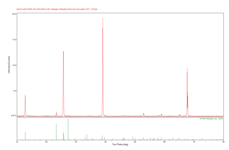
��Ʒ:Two-dimensional oxide ��-MoO3 crystal
ID��BK2020072718
CAS��
price�� $205
Item ID��BK2020072718-01
specification��
Detailed
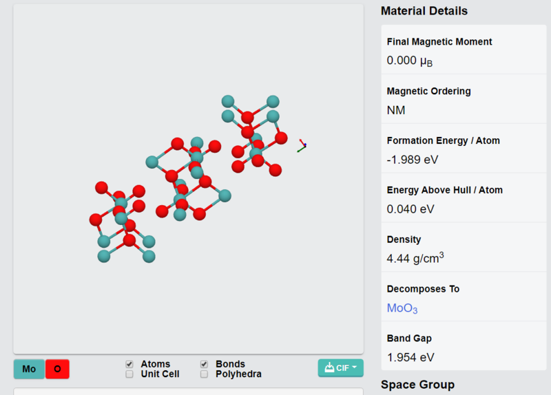
MoO3 ����
|
�������� Name |
MoO3 |
|
���ʷ��� Electrical properties |
��״������ |
|
�������� Bangap |
0 eV |
|
�ϳɷ��� Synthetic method |
CVT |
|
����ṹ Crystal Structure |
|
|
�������׳̶� Degree of difficulty for exfoliation |
���� |
|
������Ϣ�� |
����ѯ��sales@6carbon.com |
references
1�� Das, Tilak, Sergio Tosoni, and Gianfranco Pacchioni. "Structural and electronic properties of bulk and ultrathin layers of V2O5 and MoO3." Computational Materials Science 163 (2019): 230-240.
2��Dang, Yang, et al. "Solution processed hybrid Graphene-MoO3 hole transport layers for improved performance of organic solar cells." Organic Electronics 67 (2019): 95-100.
3��Li, Yungui, et al. "Ultrathin MoO3 Layers in Composite Metal Electrodes: Improved Optics Allow Highly Efficient Organic Light�\Emitting Diodes." Advanced Optical Materials 7.3 (2019): 1801262.


| Warm tip: the products supplied by Beijing Beike Xincai Technology Co., Ltd. are only used for scientific research, not for human body |
| Item ID | Info |
| BK2020072718-01 | CAS�� ID��BK2020072718 Pack�� Parameter��>10ƽ������ Stock��100 Make up�� Price��$205 |
| BK2020072718-02 | CAS�� ID��BK2020072718 Pack�� Parameter��>25ƽ������ Stock��100 Make up�� Price��$294 |
- Previous�� Two-dimensional infrar
- Next�� Few-layer NbS2 nanoshe