

 Two-dimensional material micro-nano processing - in situ testing
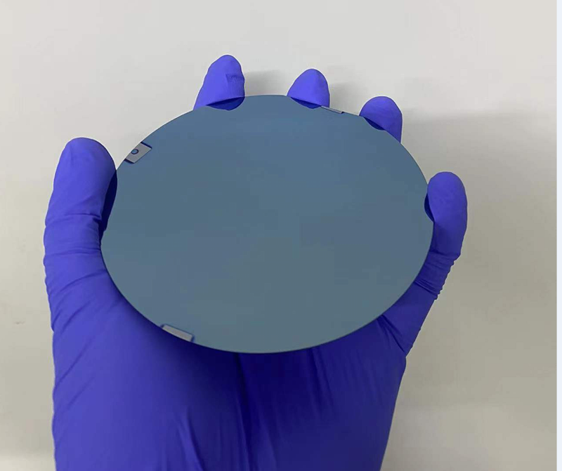
产品:Gold-plated silicon wafer for mechanical peeling
ID:BK2022051207
CAS:
price: $225
Item ID:BK2022051207-01
specification:
Detailed
Membrane material: 2nmTi+2nmAu
Silicon wafer specifications: 4 inches, single-sided polishing, double-sided oxidation, (100) crystal orientation, high conductivity N or P type optional, resistivity less than 0.1 ohm*cm-1.
Production process: cleaning> electron beam evaporation 2nmTi+1nmAu metal layer->inspection->packaging.
Packaging Specifications: Individually packaged 4 inches per piece.
Special customization: Send the demand diagram and demand quantity to sales@6carbon.com, and make a quotation after evaluating the cost and difficulty.
The above price is a reference price, please consult the technology for detailed quotation
| Warm tip: the products supplied by Beijing Beike Xincai Technology Co., Ltd. are only used for scientific research, not for human body |
| Item ID | Info |
| BK2022051207-01 | CAS: ID:BK2022051207 Pack:1片装, N型 Parameter:300nm Stock:100 Make up: Price:$225 |
| BK2022051207-02 | CAS: ID:BK2022051207 Pack:1片装, N型 Parameter:100nm Stock:100 Make up: Price:$300 |
| BK2022051207-03 | CAS: ID:BK2022051207 Pack:1片装, N型 Parameter:500nm Stock:100 Make up: Price:$300 |
| BK2022051207-04 | CAS: ID:BK2022051207 Pack:1片装,P 型 Parameter:300nm Stock:100 Make up: Price:$225 |
| BK2022051207-05 | CAS: ID:BK2022051207 Pack:1片装,P 型 Parameter:100nm Stock:100 Make up: Price:$300 |
| BK2022051207-06 | CAS: ID:BK2022051207 Pack:1片装,P 型 Parameter:500nm Stock:100 Make up: Price:$300 |
- Previous: Ga2O3 gallium oxide, g
- Next: Graphene FET (Mechanic