Nano Res.│Review of Zhang Yues team: Research progress of van der Waals structure characterization technology in two-dimensional TMDCs
QQ Academic Group: 1092348845
Detailed
Background introduction
Two-dimensional materials can be freely stacked and assembled through weak van der Waals interactions, and get rid of the severe limitations of traditional methods such as directional doping and epitaxial growth on the types of materials, allowing people to flexibly design van der Waals heterostructures with different functions. Among the many two-dimensional materials, two-dimensional transition metal chalcogenides (TMDCs) have unique electronic structures and excellent photoelectric properties. Two-dimensional van der Waals structures based on TMDCs will be used in future applications such as integrated circuits, photodetectors, and sensors. Broad prospects for development. In the limit of atomic-level thickness, the surface atomic structure and interface coupling determine the characteristics and functions of the van der Waals structure. Therefore, the development of advanced characterization technology to fully and accurately analyze the structure-activity relationship of the two-dimensional van der Waals structure is a scientific problem to be solved.
Introduction to Achievements
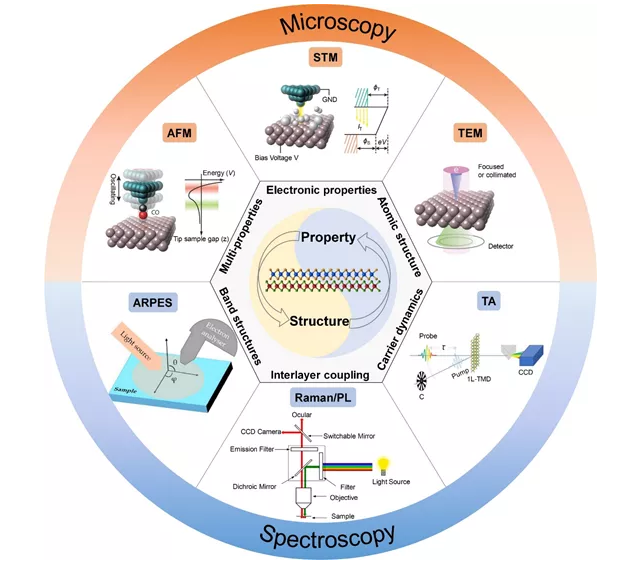
Academician Zhang Yue and Associate Professor Zhang Zheng of the University of Science and Technology Beijing focused on two-dimensional TMDCs semiconductor materials, and systematically reviewed the latest research results of advanced characterization techniques in revealing the structure-activity relationship and interface coupling properties of two-dimensional TMDCs. In this paper, starting from the stacking structure characteristics of the van der Waals heterojunctions of two-dimensional TMDCs and the matching relationship between the interface energy bands, the traditional microscopic characterization techniques (transmission electron microscope, scanning tunneling microscope and atomic force microscope) are systematically summarized in the analysis of the van der Waals structure of two-dimensional TMDCs. The research progress in the lattice structure and electronic structure of the company has paid special attention to the unique Moore superlattice structure of the two-dimensional van der Waals interface and its related characteristics. Furthermore, the Raman/Fluorescence Spectroscopy (Raman/PL), Transient Absorption Spectroscopy (TA) and Angle Resolved Photoelectron Spectroscopy (ARPES) and other spectroscopic characterization techniques were systematically discussed, aiming at the characterization of the interlayer coupling of the van der Waals structure of two-dimensional TMDCs. , Analysis of new phenomena and new principles such as interface carrier dynamics and interface band structure. Starting from the structure and physical characteristics of two-dimensional TMDs, it is proposed to promote the van der Waals material of two-dimensional TMDs from four aspects: coupling and combining multiple characterization methods, improving temporal and spatial resolution, realizing high-efficiency large-area non-destructive testing, and introducing artificial intelligence technology. The development of mass-junction characterization technology.

About the Author
Professor Zhang Yues research team from University of Science and Technology Beijing is mainly engaged in the research of low-dimensional semiconductor materials and devices. Associate Professor Zhang Zheng research team mainly focuses on the application of two-dimensional transition metal chalcogenide semiconductor materials in electronic and optoelectronic devices, targeting two-dimensional transition metal chalcogenides Research on defect engineering control mechanism of electrical performance, mixed-dimensional van der Waals heterostructure optoelectronic devices and two-dimensional logic electronic devices, and published more than 30 papers in journals such as Nature Energy, Nature Communications, Science Advances, Advanced Materials, ACS Nano, etc.; One monograph in English; 20 patent applications, 12 authorized invention patents; one second prize of the National Natural Science Award.
Two-dimensional materials can be freely stacked and assembled through weak van der Waals interactions, and get rid of the severe limitations of traditional methods such as directional doping and epitaxial growth on the types of materials, allowing people to flexibly design van der Waals heterostructures with different functions. Among the many two-dimensional materials, two-dimensional transition metal chalcogenides (TMDCs) have unique electronic structures and excellent photoelectric properties. Two-dimensional van der Waals structures based on TMDCs will be used in future applications such as integrated circuits, photodetectors, and sensors. Broad prospects for development. In the limit of atomic-level thickness, the surface atomic structure and interface coupling determine the characteristics and functions of the van der Waals structure. Therefore, the development of advanced characterization technology to fully and accurately analyze the structure-activity relationship of the two-dimensional van der Waals structure is a scientific problem to be solved.
Introduction to Achievements
Academician Zhang Yue and Associate Professor Zhang Zheng of the University of Science and Technology Beijing focused on two-dimensional TMDCs semiconductor materials, and systematically reviewed the latest research results of advanced characterization techniques in revealing the structure-activity relationship and interface coupling properties of two-dimensional TMDCs. In this paper, starting from the stacking structure characteristics of the van der Waals heterojunctions of two-dimensional TMDCs and the matching relationship between the interface energy bands, the traditional microscopic characterization techniques (transmission electron microscope, scanning tunneling microscope and atomic force microscope) are systematically summarized in the analysis of the van der Waals structure of two-dimensional TMDCs. The research progress in the lattice structure and electronic structure of the company has paid special attention to the unique Moore superlattice structure of the two-dimensional van der Waals interface and its related characteristics. Furthermore, the Raman/Fluorescence Spectroscopy (Raman/PL), Transient Absorption Spectroscopy (TA) and Angle Resolved Photoelectron Spectroscopy (ARPES) and other spectroscopic characterization techniques were systematically discussed, aiming at the characterization of the interlayer coupling of the van der Waals structure of two-dimensional TMDCs. , Analysis of new phenomena and new principles such as interface carrier dynamics and interface band structure. Starting from the structure and physical characteristics of two-dimensional TMDs, it is proposed to promote the van der Waals material of two-dimensional TMDs from four aspects: coupling and combining multiple characterization methods, improving temporal and spatial resolution, realizing high-efficiency large-area non-destructive testing, and introducing artificial intelligence technology. The development of mass-junction characterization technology.

About the Author
Professor Zhang Yues research team from University of Science and Technology Beijing is mainly engaged in the research of low-dimensional semiconductor materials and devices. Associate Professor Zhang Zheng research team mainly focuses on the application of two-dimensional transition metal chalcogenide semiconductor materials in electronic and optoelectronic devices, targeting two-dimensional transition metal chalcogenides Research on defect engineering control mechanism of electrical performance, mixed-dimensional van der Waals heterostructure optoelectronic devices and two-dimensional logic electronic devices, and published more than 30 papers in journals such as Nature Energy, Nature Communications, Science Advances, Advanced Materials, ACS Nano, etc.; One monograph in English; 20 patent applications, 12 authorized invention patents; one second prize of the National Natural Science Award.
- Previous: This Angew has identif
- Next: ACS Nano | Triplex π-c


 Academic Frontier
