

 Academic Frontier
Review: controllable preparation of graphene thin films with wafer size: challenges, current status and Prospects
QQ Academic Group: 1092348845

Detailed
Graphene has high electron mobility, thermal conductivity and excellent light transmittance, which has broad application prospects in the fields of electronics, optics and sensors; Wafer is usually the substrate of semiconductor transistor or integrated circuit, which is the basic material of semiconductor industry. The combination of graphene film and wafer materials makes it possible to fabricate graphene based device arrays by traditional micro nano processing technology. Therefore, the key to promote the industrial application of graphene based devices is to develop the preparation methods of high-quality graphene film with wafer size. Among many methods of graphene preparation, chemical vapor deposition (CVD) has the outstanding advantages of high controllability, low cost and large-scale. The graphene film prepared by CVD has high crystalline quality and has become the most important method to prepare high-quality graphene film.
Liu Zhongfan of Peking University and sun Jingyu of Suzhou University systematically reviewed the latest progress in the preparation of wafer size graphene films by chemical vapor deposition (CVD). Based on the practical application scenarios, the quality and compatibility requirements of graphene films were analyzed, and the preparation strategies were discussed based on the chemical reaction kinetics and gas phase fluid dynamics of CVD graphene, The important research directions in this field are also prospected.
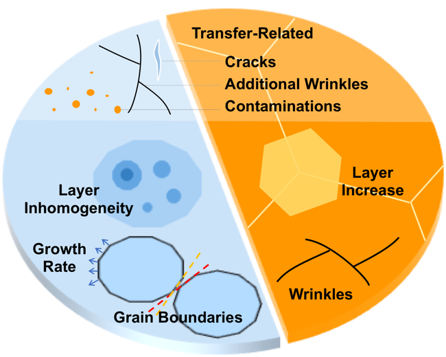
Figure 1 challenges of CVD preparation of graphene thin films with wafer size.
Starting from the application orientation, the authors systematically reviewed the quality and compatibility requirements of graphene films with different wafer sizes in different application scenarios, and summarized the challenges of CVD preparation of graphene films with wafer sizes. Then, the latest progress in the preparation of graphene thin films with wafer size is reviewed. Starting from the basic steps of chemical vapor deposition of graphene, the thermodynamics, growth kinetics and fluid dynamics are discussed respectively. The key points of the preparation of graphene thin films with wafer size are attributed to the solid and gas phases in the system, The effects of two key interfaces, the substrate surface boundary layer and the graphene substrate interface, on the growth of graphene were emphasized. The mass preparation methods of graphene thin films with wafer size were discussed from the point of view of controlling the flow field and temperature field in the reaction system. Finally, the current methods of preparing graphene thin films with wafer size by CVD are listed and summarized, and the following three aspects of the future research are put forward: a) developing CMOS compatible preparation methods; b) Development of preparation methods on amorphous substrates; c) The controllable preparation of defect rich graphene was realized.
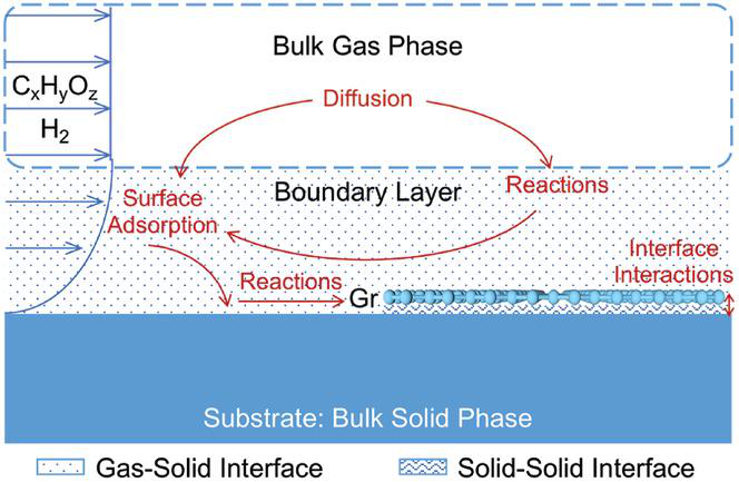
Fig. 2 growth of graphene by CVD
This information is from the Internet for academic exchange only. If there is any infringement, please contact us to delete it immediately
- Previous: The function of ACS Na
- Next: Bioactive Materials|离子