

 mxene academic
AFM: In situ formation of multiple Schottky barriers by MXene for highly sensitive gas sensors
QQ Academic Group: 1092348845
Detailed
MXene is a two-dimensional star material that is even hotter than graphene. As an advanced MXene manufacturer, BeiKonami has launched special offers, 10% off mxene and other materials, and more preferential prices, waiting for you to kill!


Two-dimensional materials have been widely used in gas sensing due to their unique properties, such as high surface-to-volume ratio, easy fabrication of chips, room temperature operation, and enhanced sensing performance from bulk to atomically thin layers. In addition, they possess special active sites such as vacancies, defects, and edge structures whose functional groups can be modified to achieve different sensing behaviors.
The gas-sensing mechanism of two-dimensional materials is mainly surface charge transfer and Schottky barrier (SB) modulation. When gas molecules are adsorbed on the surface of the material, the resistance of the material is shifted. During surface charge transfer, the interaction between gas molecules and 2D materials can lead to an increase or decrease in various resistive behaviors, depending on the dominant carriers of the semiconductor and the electron-donating/withdrawing properties of the gas molecules. This resistance change can be further enhanced by creating SBs that form at the metal and semiconductor interface. For example, strong oxidizing gases can move the SB upwards, suppressing electron transport to a large extent, yielding high gas-induced responses when the dominant mobility carriers are electrons.
Recently, Professor Seon Joon Kim and Hee-TaeJung of Korea Advanced Institute of Science and Technology (KAIST) published an article titled: In Situ Formation of Multiple Schottky Barriers in a Ti3C2 MXene Film and its Application in the internationally renowned academic journal Advanced Functional Materials A research paper in Highly Sensitive Gas Sensors, in this work, demonstrated enhanced gas sensing performance according to the formation of multiple SB sites. TiO2 crystals are formed in situ on Ti3C2 MXene, and the semiconductor/metal SB junction is realized from a single starting material by controlled oxidation. Different from previous studies on oxidized MXenes, the oxidation was performed on the assembled membrane, oxidizing the MXene flakes in aqueous solution to decorate all the MXene flakes with oxide, ensuring the maximum number of SB connections after the membrane was assembled. The gas sensing performance of the optimized TiO2/Ti3C2MXene material in the presence of NO2 gas is better than that of the pristine Ti3C2 MXene. This paper also confirmed the existence of sheet-like SB sites by direct observation by transmission electron microscopy (TEM), and verified the modulation effect of SB by comparing the sensing performance of composite Ti3C2@TiO2 films synthesized with commercial TiO2 nanoparticles.

Figure 2. XPS, XRD, Raman characterization of TiO2/Ti3C2MXene.
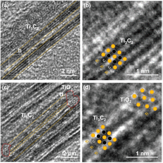
Figure 3. TEM images of Ti3C2 and TiO2/Ti3C2.

Figure 4. Gas sensing performance of the TiO2/Ti3C2 gas sensor.

Figure 5. Sensing Mechanism Expectations.

In conclusion, this paper demonstrates the in situ formation of sheet-like SBs in Ti3C2 MXene films and investigates the enhancement of gas sensing performance depending on the strength of the SB site. The possibility of utilizing SB sites to enhance the gas sensing performance of these films is verified, for example when strong oxidizing gases like NO2 are used to greatly tune the position of SBs. The gas response of the optimally synthesized TiO2/Ti3C2MXene gas sensor is 13.7 times higher than that of the pristine Ti3C2 gas, reaching the detection limit of 125 ppb NO2 gas at room temperature, indicating the improved sensitivity of the TiO2/Ti3C2 MXene gas sensor. Our new strategy achieves fine control over SB modulation and maximizes the density of SB junctions within a single gas sensing channel, proposing a simple approach to improve gas sensing performance.


Two-dimensional materials have been widely used in gas sensing due to their unique properties, such as high surface-to-volume ratio, easy fabrication of chips, room temperature operation, and enhanced sensing performance from bulk to atomically thin layers. In addition, they possess special active sites such as vacancies, defects, and edge structures whose functional groups can be modified to achieve different sensing behaviors.
The gas-sensing mechanism of two-dimensional materials is mainly surface charge transfer and Schottky barrier (SB) modulation. When gas molecules are adsorbed on the surface of the material, the resistance of the material is shifted. During surface charge transfer, the interaction between gas molecules and 2D materials can lead to an increase or decrease in various resistive behaviors, depending on the dominant carriers of the semiconductor and the electron-donating/withdrawing properties of the gas molecules. This resistance change can be further enhanced by creating SBs that form at the metal and semiconductor interface. For example, strong oxidizing gases can move the SB upwards, suppressing electron transport to a large extent, yielding high gas-induced responses when the dominant mobility carriers are electrons.
Recently, Professor Seon Joon Kim and Hee-TaeJung of Korea Advanced Institute of Science and Technology (KAIST) published an article titled: In Situ Formation of Multiple Schottky Barriers in a Ti3C2 MXene Film and its Application in the internationally renowned academic journal Advanced Functional Materials A research paper in Highly Sensitive Gas Sensors, in this work, demonstrated enhanced gas sensing performance according to the formation of multiple SB sites. TiO2 crystals are formed in situ on Ti3C2 MXene, and the semiconductor/metal SB junction is realized from a single starting material by controlled oxidation. Different from previous studies on oxidized MXenes, the oxidation was performed on the assembled membrane, oxidizing the MXene flakes in aqueous solution to decorate all the MXene flakes with oxide, ensuring the maximum number of SB connections after the membrane was assembled. The gas sensing performance of the optimized TiO2/Ti3C2MXene material in the presence of NO2 gas is better than that of the pristine Ti3C2 MXene. This paper also confirmed the existence of sheet-like SB sites by direct observation by transmission electron microscopy (TEM), and verified the modulation effect of SB by comparing the sensing performance of composite Ti3C2@TiO2 films synthesized with commercial TiO2 nanoparticles.


Figure 2. XPS, XRD, Raman characterization of TiO2/Ti3C2MXene.
Figure 3. TEM images of Ti3C2 and TiO2/Ti3C2.
Figure 4. Gas sensing performance of the TiO2/Ti3C2 gas sensor.
Figure 5. Sensing Mechanism Expectations.
In conclusion, this paper demonstrates the in situ formation of sheet-like SBs in Ti3C2 MXene films and investigates the enhancement of gas sensing performance depending on the strength of the SB site. The possibility of utilizing SB sites to enhance the gas sensing performance of these films is verified, for example when strong oxidizing gases like NO2 are used to greatly tune the position of SBs. The gas response of the optimally synthesized TiO2/Ti3C2MXene gas sensor is 13.7 times higher than that of the pristine Ti3C2 gas, reaching the detection limit of 125 ppb NO2 gas at room temperature, indicating the improved sensitivity of the TiO2/Ti3C2 MXene gas sensor. Our new strategy achieves fine control over SB modulation and maximizes the density of SB junctions within a single gas sensing channel, proposing a simple approach to improve gas sensing performance.
- Previous: AFM: Polysiloxane Cros
- Next: Bioactive Materials |