

 Academic Frontier
Hunan University‘s latest Nature: a universal synthesis method for two-dimensional heterostructure arrays
QQ Academic Group: 1092348845

Detailed
【introduction】
Although the application prospects of two-dimensional materials are very broad, how to greatly increase the yield of two-dimensional materials such as van der Waals heterostructures has been one of the main difficulties hindering their development. At present, the main method for preparing two-dimensional van der Waals heterostructures is still micromechanical exfoliation―a synthetic method that cannot effectively increase yield. Therefore, the search for new methods for mass production is still a hot topic in the field of two-dimensional materials.
[Achievement Profile]
Recently, Duan Zhuofeng of the University of California, Los Angeles, and Duan Xidong of Hunan University (co-corresponding author) and others have jointly reported that a two-dimensional van der Waals can be prepared using metallic transition metal sulfides and semiconductor transition metal sulfides A General Synthesis Strategy for Heterostructure Arrays. By selectively patterning nucleation sites on single- or double-layer semiconductor transition metal sulfides, researchers have precisely controlled the nucleation and growth of a variety of metallic transition metal sulfides. These metallic transition metal sulfides all have a programmable periodic arrangement and lateral dimensions that can be adjusted in specified areas, and can eventually form a series of van der Waals heterogeneous arrays. Further experiments show that this synthesis strategy can prepare transistor devices with excellent performance and high yield, which provides new ideas for mass production of high-performance new devices. On March 11, 2020, the relevant results were published online in Nature with an article entitled "General synthesis of two-dimensional van der Waals heterostructure arrays".
[Picture and text guide]
Figure 1 Schematic diagram of the growth process
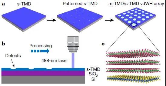
Figure 2 Characterization of VSe2 / WSe2 Van der Waals heterogeneous array
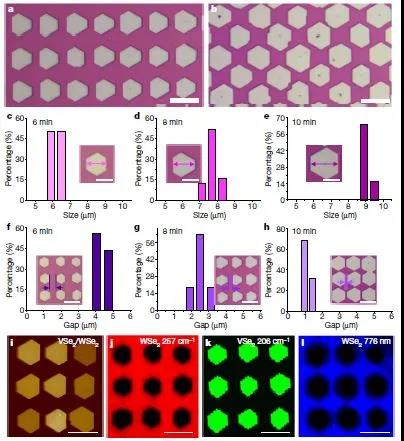
Fig.3 Nucleation growth mechanism of VSe2 on patterned WSe2
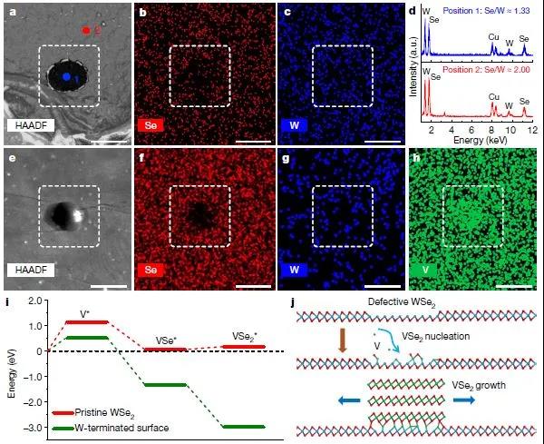
Fig. 4 Electron microscopy characterization of VSe2 / WSe2 van der Waals heterostructure

Figure 5 Characterization of CoTe2 / WSe2 and NiTe2 / WSe2

Figure 6.Electrical characterization of VSe2 / WSe2 van der Waals heterogeneous array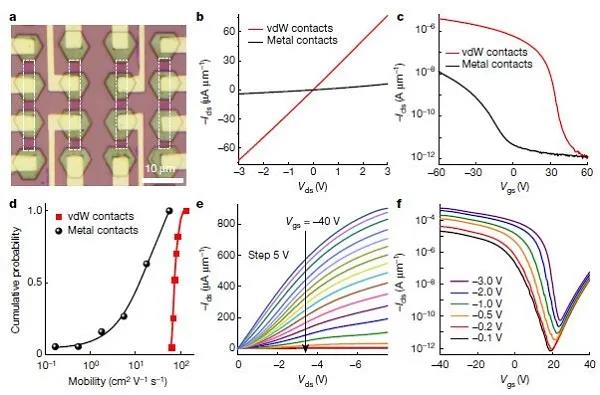
Literature link: General synthesis of two-dimensional van der Waals heterostructure arrays (Nature, 2020, DOI: 10.1038 / s41586-020-2098-y)
Source of information: material source
- Previous: Carding: An Overview o
- Next: Bioactive Materials|离子