

 Academic Frontier
Explore the optical behavior of high-density and randomly distributed nanowire arrays
QQ Academic Group: 1092348845
Detailed
| Vertical semiconductor nanowire arrays are promising materials for retinal repair and can help restore the eyesight of people with severe retinal diseases. These nanowires can also be used to make bio-inspired photoreceptors and lightweight and efficient photovoltaic cells. | |
| "Many studies based on the next generation of semiconductor optoelectronic vertical nanowire implemented nanowires are concentrated in the collective optical characteristic and device performance, these phenomena can be observed and demonstrated on a macroscopic scale," Associate Professor, School of the Young Min Song Gwangju Nannank, head of the Department of Electrical Engineering and Computer Science at the Institute of Technology, explained. "Although the individual resonance of the combined nanowires triggers macroscopically observable optical properties, the detailed photon phenomenon in nanowire arrays has not been studied so far." | |
| In fact, novel and interesting photon events (such as strong absorption, scattering, and wavelength selectivity) are caused by individual resonances of the nanowires, which are called guided (or leaked) modes. | |
| In the latest research results of the Song group ( published in " Advanced Optical Materials" ( "Selective and Sensitive Photon Sieves Based on Forests of III-V Semiconductor Nanowires Made by Non-lithography Process" )), scientists raised Theoretical and experimental research on the optical behavior of optical microscopes. Dense and randomly distributed arrays of nanowires embedded in transparent polymers are called selective and sensitive photon sieves (SSPS). | |
| They found that under certain geometric parameters, random and dense III-V nanowire forests can have resolvable nano-optical resonances in response to different incident photons. | |
| Song pointed out: "Our experimental observations also successfully supported our calculation results by displaying unique spectral images that depend on wavelengths (including blue, green, red, and near-infrared colors)." | |
|
|
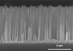
| SEM image of vertical nanowire array. (Reprinted with permission from Wiley-VCH Verlag) | |
| In the past few years, Song’s group has focused on developing optical filters based on semiconductor nanowires and imaging devices inspired by biology. | |
| He said: “Based on our previous research, we are naturally interested in the spectral response of vertical nanowire arrays, which is similar to biological retinal cells.” “We provide affordable methods by growing samples without using nanolithography To thoroughly study the optical events of the vertical nanowire array and embed the sample in a transparent polymer." | |
| The team also developed a design guide for using vertically aligned III-V nanowire forests as artificial photoreceptors. This research may help to develop artificial eyes and high-resolution cameras inspired by biology. | |
| Particularly attractive for retinal prosthesis applications is the high photon selectivity and sensitivity in the broadband range from ultraviolet, visible and near infrared. Furthermore, the flexibility of the nanowires and encapsulating polymer allows the prosthetic device to be integrated with the damaged or blind retina. | |
|
|
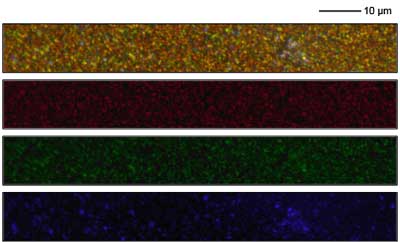
| Selective and sensitive photon sieves (SSPS) have different spectral responses to white, red, green, and blue light. (Photo: Song Research Group) | |
| At this stage of their work, the researchers demonstrated that a randomly dense forest of nanowires can spectrally distinguish incident photons in a single nanowire with high absorption. In order to develop an artificial photoreceptor, the next step is to connect metal electrodes to each nanowire in order to read individual electrical signals from them. | |
| Song concluded: "We need a novel electrical connection and data reading strategy so that we can build functional devices." "It is not easy to make separate electrical connections with a large number of nanowires, but we believe that submicron Cutting-edge, complementary metal oxide semiconductor (CMOS) circuit technology is a potential solution to this problem." |
- Previous: Professor Li Run of Hu
- Next: Bioactive Materials|离子