

 Academic Frontier
Interpretation of nanomaterials-how quantum dots can make the world more exciting
QQ Academic Group: 1092348845
Detailed
Quantum dots are quasi-zero-dimensional nanomaterials that bind excitons in three dimensions. Roughly speaking, the three dimensions of quantum dots are all below 100nm, and their appearance is generally spherical or quasi-spherical, so they are also called nanocrystals. Scientists have invented many different methods to manufacture quantum dots, such as chemical solution growth method, epitaxial growth method and electric field confinement method. The quantum dots prepared by the chemical solution growth method are mostly colloidal, which have the advantages of low cost, high yield, and high luminous efficiency, but their electrical conductivity is low, which greatly limits their application in electrical devices; the epitaxial growth method is one This is a method of nucleating and growing quantum dots on a substrate material. The quantum dots grown by this method can be easily combined with traditional semiconductor devices. In addition, it has higher charge transfer efficiency and fewer surface defects. However, due to the need for high vacuum or ultra-high vacuum during the reaction, the cost of quantum dots prepared by this method is relatively high; the electric field confinement method is a method of adjusting the potential of the metal electrode The energy level in the semiconductor is distorted to form a method of preparing quantum dots by constraining carriers. The cost is the highest and the yield is the lowest. However, due to the extremely high controllability, the quantum dots produced by this method are widely used in the research of quantum computing theory.
The discovery of quantum dots was named one of the ten scientific breakthroughs of the year by Science magazine in 2003. After more than ten years of development, quantum dots have been widely used in solar cells, medical testing, displays, and other fields due to their excellent physical, optical, and electrical properties. The author has collected some recent application papers of quantum dots, hoping to inspire them.
Display field

Quantum dot light-emitting diodes (QLEDs) show excellent application prospects in the field of optical lighting and displays due to their higher color saturation, brightness, spectral tunability and low dispersion. Luminous brightness, external quantum efficiency and lifetime are the three major indicators of QLED‘s practical application. Existing research results show that: for quantum dot light-emitting diodes, high brightness and high external quantum efficiency (EQE) are difficult to achieve at the same time. How to prepare QLEDs with high brightness, high external quantum efficiency and long life is a hot research topic.
The research group of Du Zuliang and Li Linsong of Henan University and the research group of Zhang Zhenyu of University of Science and Technology of China reported a CdSe/ZnSe core/shell structured quantum dot with high brightness and high external quantum efficiency. The highest brightness of the obtained red, green, and blue QLED devices are 356000 cd/m2, 614000 cd/m2 and 62600 cd/m2 respectively, the highest external quantum efficiency is 21.6%, 22.9% and 8.05%, and the red and The life of the green device is 1,600,000 h, and the life of the blue device is 7,000 h. [1] Related research was published in Nature Photonics with the title "Visible Quantum Dot Light-emitting Diodes with Simultaneous High Brightness and Efficiency".
01
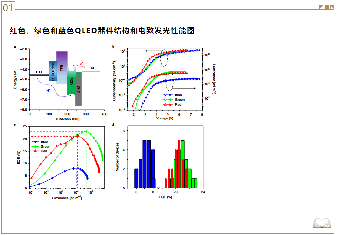
Red, green and blue QLED device structure and electroluminescence performance graph
In order to reduce the use of toxic element cadmium in light-emitting diodes, light-emitting diodes based on indium phosphide have been developed, but their performance is relatively poor and cannot meet the needs of practical applications. Recently, the Eunjoo Jang team of Samsung Advanced Technology Research Institute in South Korea used hydrofluoric acid to etch and oxidize the surface of the InP core during the growth of the initial ZnSe shell, and then realized the growth of ZnSe at a high temperature of 340 ℃, thereby preparing InP / ZnSe / Znhe core-shell structure of quantum dots, and the yield is about 100%. The light-emitting diode prepared based on the quantum dot shows the theoretical maximum external quantum efficiency (21.4%), and its brightness can reach 100,000 cd m-2. In the case of 100cd m-2, it can be used for 1000000 h, showing excellent stability, and its performance is similar to the latest cadmium-containing QLED, showing great commercial value. [2] Related research was published in Nature with the title of "Highly efficient and stable InP/ZnSe/ZnS quantum dot light-emitting diodes".
02
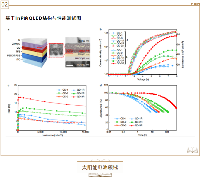
InP-based QLED structure and performance test chart
Solar cell field
Defect passivation and surface modification of perovskite hybrid films are essential for achieving high power conversion efficiency (PCE) and stable perovskite photovoltaics. The existence of defects traps charge carriers and inhibits quasi-Fermi level splitting, thereby reducing the open circuit voltage (VOC) of perovskite solar cells. At the same time, the existence of defects can cause catalytic degradation due to rapid ion migration. Therefore, surface modification aimed at reducing defect density and preventing ion migration is of interest for improving the stability of perovskite solar cells. Common strategies include the introduction of metal ions, surface and interface modification, heterojunction engineering, and the addition of functional additives. In addition to defect passivation-based strategies, molecular surface functionalization methods that make perovskite membranes waterproof and inhibit ion migration also make significant contributions to improving the stability of the device. Studies have found that inorganic perovskite quantum dots with a large number of elements and capped ligands are very attractive for element passivation and molecular surface functionalization.
Recently, Prof. Osman M. Bakr’s research group from King Abdullah University of Science and Technology reported on the use of trace ligand-terminated CsPbBrCl2 QDs as transfer elements and molecular surface modifiers to improve the PCE and stability of MAPbI3 solar cells The easy way. These doped MAPbI3 solar cells show reduced tail states, smaller trap density and longer carrier lifetime, which in turn increases the VOC of the MAPbI3 planar heterojunction device, thus increasing the PCE to 21.5%. At the same time, due to the self-assembly properties of the ligand, the surface of MAPbI3 is finally closed, so the stability of MAPbI3 is greatly improved. These results highlight the importance of the synergistic effect of element passivation and surface modification for improving the efficiency and stability of titanium ore solar cells. [3] The related research was published in Joule with the title of "Quantum Dots Supply Bulk- and Surface-Passivation Agents for Efficient and Stable Perovskite Solar Cells".
03
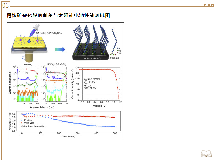
Preparation of perovskite hybrid film and solar cell performance test chart
Organic solar cells (OSC) are flourishing in the photovoltaic field with low cost, flexibility and competitive power conversion efficiency (PCE). However, compared with inorganic or hybrid solar cells, the performance of OSC is limited, partly because of the limited daylighting provided by the receptor bulk heterojunction (BHJ) mixture. Therefore, there is still a need to improve OSC performance. A relatively common strategy is to incorporate the third optically active component into the binary BHJ blend. Because it has the potential to further modulate the photoelectric and morphological characteristics of the traditional BHJ active layer, it has caused more and more attention. Recently, the Kevin Sivula research group of the Federal Institute of Technology in Lausanne prepared a lead halide perovskite quantum dot (LHP QD) with solution processability, excellent photoelectric properties, and cheap and easy availability, and applied it to the ternary OSC. In preparation. The ternary OSC preparation process is as follows: by integrating CsPbI3 QD into a conventional organic solar cell (OSC) and embedding LHP QD in a donor-acceptor (PTB7-Th: PC71BM) bulk heterojunction. By optimizing the mass load to 3%, its power conversion efficiency can reach 10.8%, performance has increased by 35%, and it has set a record for hybrid ternary OSC. The study of the mechanism shows that the increase in exciton separation and the decrease in recombination in the receptor phase are the main reasons for the enhanced performance. [4] Related research was published in Angewandte Chemie with the title "Lead Halide Perovskite Quantum Dots To Enhance the Power Conversion Efficiency of Organic Solar Cells".
04
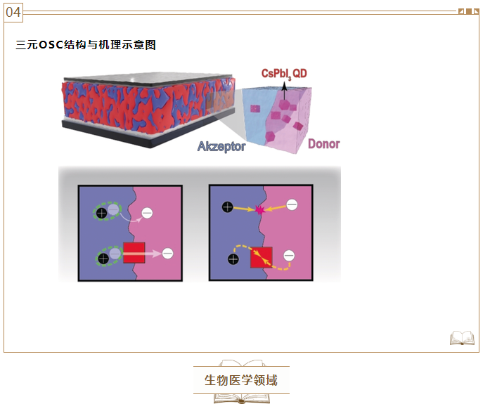
Schematic diagram of ternary OSC structure and mechanism
Biomedical field
In the past few years, two-dimensional (2D) transition metal dichalcogenides (TMD) with a similar structure to graphene have attracted great attention. Due to the characteristics of its own band gap semiconductor, it has inspired applications in biomedicine, sensors, transistors, catalysts, photodetectors and energy storage devices. The lateral size of several-layer or single-layer TMD nanosheets is further reduced to become quantum dots (QD), and their electrical/optical properties are further enhanced due to their stronger quantum confinement and edge effects. At this stage, how to prepare biocompatible and low-cost TMD quantum dots has become a difficult point. Recently, the Chwee Teck Lim and David Tai Leong research groups of the National University of Singapore adopted a bottom-up approach, using TM oxides or chlorides and chalcogen precursors to rapidly synthesize a variety of materials under mild aqueous and room temperature conditions. TMD quantum dots (MoS2, WS2, RuS2, MoTe2, MoSe2, WSe2 and RuSe2). By deviating the reaction stoichiometric ratio of the precursor from its fixed molecular stoichiometric ratio, an adjustable defect state can be achieved in the same reaction. The prepared MoS2 quantum dots were used in biomedical applications, and the results showed that the sulfur defects in the MoS2 quantum dots enhanced the production of oxidative stress in cancer cells through photodynamic effects. [5] Related research was published in Nature Communications with the title of "Defect Engineered Bioactive Transition Metals Dichalcogenides Quantum Dots".
05
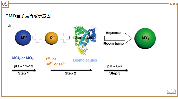
Schematic diagram of TMD quantum dot synthesis
The development of a multifunctional therapeutic and diagnostic (hyperthermia) nano-platform is essential for solving challenging problems related to cancer. The research group of Professor Dongling Ma from the National Academy of Sciences of Canada has developed self-assembled super-nanoparticles composed of superparamagnetic Fe3O4 nanoparticles and photoluminescent PbS/CdS quantum dots with emission peak in the second biological window (II-BW). The self-assembled Fe3O4 and PbS/CdS (II-BW) ultra-nanoparticles [SASNs (II-BW)] exhibit excellent photoluminescence properties, which can be detected through tissues with a thickness of up to 14 mm. -Severe extinction in BW and subsequent autofluorescence is achieved. Due to the greatly improved magnetic field inhomogeneity, it shows higher T2 relaxivity (282 mM–1 s–1, which is about 4 times higher than that of free Fe3O4 nanoparticles). On the other hand, SASN (II-BW) can act as either a magnetocaloric agent or a photothermal agent, thus overcoming the shortcomings of each heating method. When SASN (II-BW) is exposed to dual-mode (magnetic and photothermal) heating, the heat transfer efficiency is 7 times that of heating alone. These results show that it has excellent light and colloidal stability and negligible cytotoxicity, which proves the potential use of SASN (II-BW) in imaging of deep tissues (magnetic resonance and photoluminescence) in vivo. It also provides SASN (II-BW) -BW) Mediated amplification of the possibility of dual-mode thermal treatment of cancer. [6] The related research was published in ACS Nano with the title of "Multifunctional Self-Assembled Supernanoparticles for DeepTissue Bimodal Imaging and Amplified Dual-Mode Heating Treatment".
06
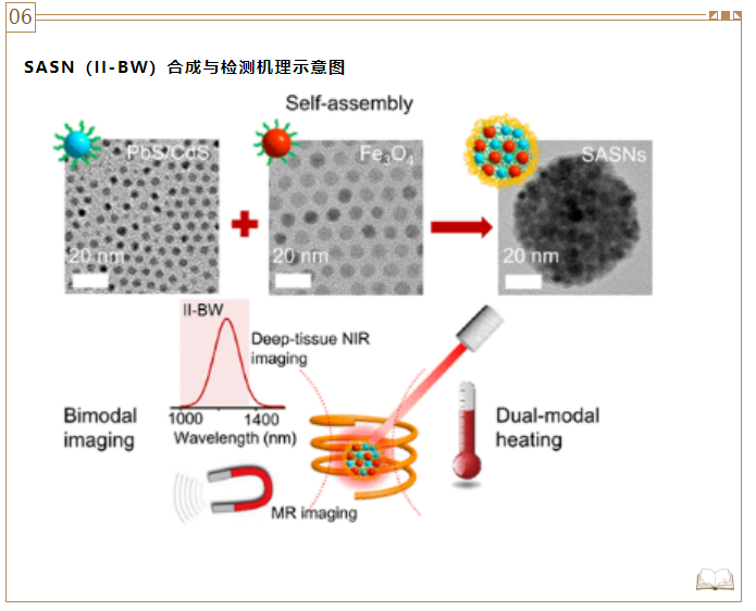
Schematic diagram of SASN (II-BW) synthesis and detection mechanism
This information is sourced from the Internet for academic exchange only. If there is any infringement, please contact us to delete it immediately.
references:
1. Shen H, Gao Q, Zhang Y, et al. Visible quantum dot light-emitting diodes with simultaneous high brightness and efficiency[J]. Nature Photonics, 2019, 13(3): 192-197.
- Previous: Study on the network s
- Next: Bioactive Materials|离子