
Research Background
Two-dimensional (2D) materials offer many interesting properties that can be used in future and existing technologies. One of the main bottlenecks in their successful integration into practical applications is the need for reproducible large-scale growth of high-quality materials. Therefore, the CVD growth of single-layer and few-layer atomic films has been extensively studied, especially transition metal chalcogenides (TMDCs). Despite great progress, metal-oxide-based CVD growth has some obvious shortcomings, which are not conducive to the study of the growth mechanism of such materials and the consistent and reasonable growth of large-area 2D atomic layers with the required thickness and chemical composition .
Introduction
In view of this, recently, Ariel Ismach and others at Tel Aviv University, Israel, reported a growth-etch MOCVD (GE-MOCVD) method to prepare the WS2 atomic layer, in which a small amount of water vapor is introduced during the growth process and the precursor is delivered in pulses. Studies have shown that the growth and evolution of the WS2 atomic layer varies with the amount of water vapor, the number and type of cycles, and the gas composition. Compared with the traditional process, this method can significantly increase the crystal domain size. Through Raman spectroscopy, photoluminescence (PL) spectroscopy and HRTEM studies, the crystal quality of WS2 (and WSe2) domains has been improved. In addition, time-resolved PL studies have shown that the exciton lifetime of the WS2 atomic layer obtained by this method is very long, comparable to that observed in mechanically peeled sheets. Therefore, the GE-MOCVD method reported in this article is expected to achieve a wide range of applications. The article was published on the famous journal ACS Nano with the title of Growth-Etch Metal-Organic Chemical Vapor Deposition Approach of WS2 Atomic Layers.
Graphic guide
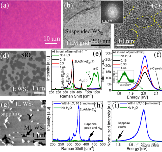
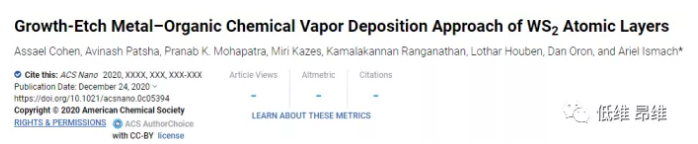
Figure 1. MOCVD growth of WS2 atomic layer with and without H2O vapor. (A-c) Results obtained for standard growth without water vapor. (D-f) On SiO2/Si substrate, the water vapor of WS2 layer assists MOCVD growth. (G-i) H2O assisted MOCVD growth on c-plane sapphire.
Figures 1a-c show the results of standard MOCVD growth of WS2 films, where W(CO)6 and di-tert-butyl sulfide (DTBS) are used as metal and chalcogen precursors, respectively. Standard MOCVD refers to a process in which the precursor flows continuously without adding water vapor. Figure 1a shows an optical micrograph of a continuous layer grown on a SiO2/Si substrate, which looks uneven. In addition to the WS2 peak, amorphous carbon (a-C) is often detected, as shown in Figure 1(f). Carbon pollution is most likely to come from organic metal (W(CO)6) and organic sulfur (DTBS) precursors. The residual amount of a-C may not have a significant impact on the growth of conventional thin film materials. However, it is essential to control the growth of 3-atom thick semiconductors (such as 2D TMDCs). Figures 1b and c show the low magnification TEM image and HRTEM image of WS2, respectively, in which the crystal lattice of the nanocrystalline (domain size of tens of nanometers) film is observed. The fast Fourier transform (FFT) clearly shows the polycrystalline pattern , Proved the nanocrystalline nature of the WS2 film. This is in good agreement with reports of TMDC layers grown by MOCVD, where the observed crystal domain size is as high as ~200 nm. Only when metal halides are added to the system can larger crystal domains be obtained in the MOCVD process. This undesirable carbon deposition has many harmful effects, such as serving as a nucleation center, thereby increasing the nucleation density (and reducing the crystal domain size), and generally contaminates the growth substrate, the surface and edges of the crystal domain.
To reduce this adverse effect, a small amount of controlled water vapor (~300 ppm) is introduced into the growth chamber. Figure 1d shows the SEM image of WS2 grown on SiO2/Si with the addition of 0.16 mmol/min water. Figures 1e and f respectively show the Raman and PL spectra of WS2 domains under different water vapor flow rates, and the peak intensity increases obviously with the increase of H2O flow rate. Similar results were obtained on sapphire, with SEM images highlighting single layer (1L), multiple layer (ML) and uncovered areas (Figure 1g). When water was added to the growth, the Raman spectrum (Figure 1h) and PL spectrum (Figure 1i) of the sample showed higher intensity, and the Raman characteristics of amorphous carbon disappeared. The lack of detectable a-C and the significant increase in Raman and PL intensities clearly indicate an increase in the crystallinity and purity of the layer. This effect can be explained by the reaction of H2O and a-C and its re-evaporation, which not only cleans the areas not covered by the growth substrate, but also cleans the crystal domains. However, due to the presence of surface impurities and the partial pressure of the precursor, this growth method does not significantly change the size of the crystal domains. Therefore, it is necessary to partially suppress the nucleation center to allow the crystal domain to expand and grow over a larger area. In order to achieve this goal, a pulse growth method was carried out. Metal and chalcogen precursors are supplied to the system in pulses (growth step), while Ar and water vapor flow continuously (etching step).
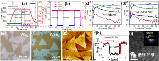
Figure 2. Growth-etch MOCVD method. (A&b) Flow and time chart of GE-MOCVD growth. (C&d) TOF-SIMS depth profile recorded from standard MOCVD and GE-MOCVD grown samples. (E&f) Typical OM images of WS2 and WSe2 grown on c-plane sapphire. (G&h) Topography and corresponding height profile. (I) Atom-resolved HADDF-STEM image of WS2 single crystal domain.
Figure 2 shows the results obtained by the GE-MOCVD method, and the gas flow changes with time are shown in Figures 2a and b. In order to further verify the reduction of carbon content on the growth substrate after the GE-MOCVD method, time-of-flight secondary ion mass spectrometry (TOF-SIMS) depth profiles were recorded on samples grown on standard MOCVD and GE-MOCVD. Compared with the GE-MOCVD sample, the a-C content detected on the standard MOCVD sample is nearly 2 orders of magnitude higher (Figure 2c and d). The typical OM images of WS2 and WSe2 (Figure 2e and f) show a significant increase in crystal domain size. The AFM topography of the original WS2 atomic layer shows a single-layer crystal domain with a thickness of ~0.77 nm (Figure 2g and h). The atomic resolution HAADF-STEM image and SAED pattern show that the crystal domain has high crystallinity (Figure 2i). The water vapor reacts with solid carbon pollutants to generate CO gas (and possibly CO2), causing it to evaporate again, thus cleaning the substrate and crystal domains, and significantly improving the size and quality of crystal domains.

Figure 3. The effect of H2O concentration on the growth of GE-MOCVD. (A-c) Typical OM images of the WS2 atomic layer grown when the H2O concentration increases. (D-f) Corresponding crystal domain size distribution. (G) Comparison of PL spectra. (H) The variation of PL fwhm and crystal domain size with H2O concentration.
The effect of H2O flow rate on growth is summarized in Figure 3. Figures 3a-c show optical images, describing the variation of crystal domain size with H2O flow rate (0.1 to 10 mmol/min), and the corresponding crystal domain size distribution is shown in Figure 3d-f. As the H2O flow rate increases, the PL intensity increases, and the full width at half maximum (fwhm) decreases (Figure g). The crystal domain size increased by more than 2 orders of magnitude, from ~0.09±0.04 μm to 11.5±2.1 μm (Figure 3h). The gradual enhancement of PL emission and the visible increase in crystal domain size clearly indicate that the optical quality and crystallinity have been significantly improved.
Figure 4. The effect of cycle number and type on growth. (A-d) The relationship between crystal domain evolution and period type. (E-g) SEM, AFM and OM images of the complete single-layer WS2 obtained with the "4G+3E" cycle. (H) The relationship between area coverage and crystal domain size and the number and type of cycles.
The microscopic images of WS2 crystal domains grown with different period types 1G, 1G+1E, 2G+1E and 3G+2E are shown in Fig. 4a-e, showing that the crystal domain size gradually increases. Figures 4e-g show the fully covered WS2 monolayer obtained using the 4G+3E cycle type. The relationship between the coverage of the WS2 atomic layer and the crystal domain size with the number and type of cycles is shown in Figure 4h. These two parameters can be controlled by cycle design to achieve a large crystal domain size of ~12 μm and coverage (100%). ).
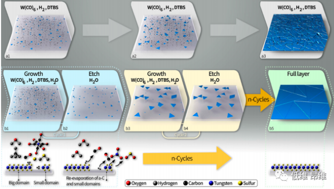
Figure 5. Schematic diagram of the growth mechanism in the standard MOCVD and GE-MOCVD methods.
The introduction of a small amount of H2O and growth precursor pulse delivery during the growth process has two main functions: First, it can eliminate or significantly reduce carbon impurities in the film and on the growth substrate, thereby obtaining a purer and higher quality WS2 film. Since the amorphous carbon on the substrate can serve as a nucleation center, simply eliminating it can result in a smaller nucleation density and thus a larger crystal domain. Secondly, H2O will etch and re-evaporate TMDCs. Therefore, the small amount of water vapor in the system reacts with some small/defective WS2 nucleation points/domains, causing them to re-evaporate, thereby reducing the nucleation density. Therefore, the most relevant reaction occurs in the etching step , where the substrate and growth area are exposed to water vapor, but not to metal and chalcogen precursors. These reactions result in the re-evaporation of carbon contaminants and small or defective WS2 domains. The schematic model of the growth process in the standard and GE-MOCVD is summarized in Figure 5.
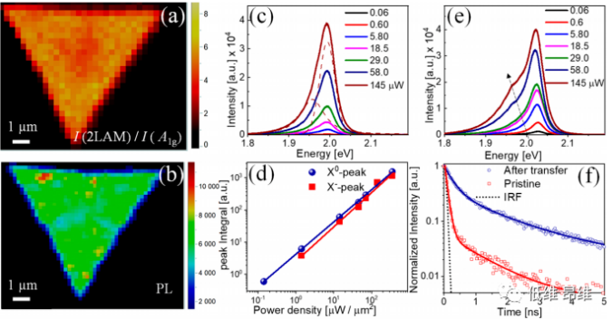
Figure 6. (a&b) Spectral imaging of Raman intensity ratio and PL intensity of single crystal WS2 domains in 2LAM and A1g modes, showing uniform single-layer characteristics. (C) The steady-state power-dependent PL spectrum of the original monolayer WS2 domain. (D) PL peak intensity changes with excitation power. (E) The steady-state power-dependent PL spectrum of the transferred monolayer WS2 domain. (F) Measured TRPL attenuation trajectories of original and transferred single crystal WS2 domains.
The Raman imaging of the intensity ratio of the 2LAM and A1g phonon modes is shown in Fig. 6a, which shows that the intensity ratio over the entire crystal domain is greater than 4, which proves the monolayer nature of WS2. In addition, the uniform optical quality of single crystal WS2 domains can be clearly seen from the uniform PL emission related to the A exciton (Figure 6b). Through the steady-state power-dependent PL and time-resolved PL (TRPL) measurements of single crystal WS2 domains, the optical quality of the original domain and the transferred WS2 domain can be further studied. The variation of the PL of the original WS2 single crystal domain with excitation power is shown in Fig. 6c, showing an emission of about 2.0 eV. As the excitation power increases, a slight asymmetric broadening also appears on the low energy side of the peak. The peak centered at ~1.99 eV was identified as neutral A exciton (X0) emission, while the low-energy peak near 1.96 eV was attributed to electron-bound exciton (negative triplet X-) emission. At all incident excitation powers, neutral exciton emission is stronger than triplet emission. In the logarithmic-logarithmic diagram (Figure 6d), two emission peak power (P)-dependent PL integrated intensities are plotted, and both exhibit linear behavior, which confirms that there is no trap-assisted compounding effect in the intermediate band gap state. The PL spectrum of the transferred WS2 single crystal domain showed an emission of about 2.02 eV at low excitation power (Figure 6e). The intensity of PL emission increases as the excitation power increases, and there is no obvious shift in the peak center. However, the broadening and intensity of the low-energy tail also increase with the increase of excitation power and evolve into a clear peak centered at ~1.95 eV. Compared with the original sample, the center of the emission peak of neutral A exciton (X0) is 2.02 eV and blue shifted (30 meV), which may be due to the strain relaxation after transfer from the growth substrate. It is worth noting that as the excitation power increases, no significant shift in X0 emission is observed. However, the low-energy triplet emission (X-) peak is red-shifted from 2.0 eV to 1.97 eV, indicating that the emission is due to electron-bound excitons ( Triplet) compound. By using TRPL to study exciton dynamics, the high optical quality of single crystal WS2 domains grown by GE-MOCVD technology is further confirmed. Figure 6f shows the TRPL spectra of the two samples at a pump flux of ~5 nJ・cm-2. This significant slowdown of non-radiative recombination highlights the significant reduction in defect states, further confirming that the WS2 atomic layer grown by GE-MOCVD technology has high optical quality.
Summary and outlook
In this paper, a growth-etch MOCVD method is developed to synthesize high optical quality WS2 (and WSe2) atomic layers. Carbon pollution that often occurs when metal-organic and organic sulfide (and selenide) precursors are used in standard MOCVD can be eliminated by sequential growth and etching processes, in which the precursors are delivered to the system in pulses, and there is continuous A small amount of water vapor. Through the re-evaporation of carbon contaminants and small and defective TMDC nucleation sites, the ultra-high nucleation density normally obtained in standard MOCVD is highly suppressed. Therefore, this method can improve crystallinity and reduce pollution. Raman spectroscopy, steady-state and time-resolved PL spectroscopy studies have proved that the crystal quality and optical quality of the atomic layer grown by GE-MOCVD have been improved. The large-scale growth of high-quality atomic films is a prerequisite for its integration into a wide range of applications. The research work in this article is an important step to achieve this goal.
Literature information
Growth-Etch Metal-Organic Chemical Vapor Deposition Approach of WS2 Atomic Layers
(ACS Nano, 2020, DOI:10.1021/acsnano.0c05394)
Literature link: https://pubs.acs.org/doi/10.1021/acsnano.0c05394
Information source: Ripper123
This information is from the Internet for academic exchanges. If there is any infringement, please contact us and delete it immediately


