 Author:
Zhongwei Wu, Peng Li, Jie Zhao, Ting Xiao, Hong Hu, Peng Sun, Zehan Wu,Jianhua Hao, Chunlin Sun, Haoli Zhang, Zhifeng Huang,* and Zijian Zheng
Introduction
Due to the high power conversion efficiency (PCE) and inherent flexibility of perovskite materials, organic metal halide perovskite solar cells (PSC) are expected to be applied to flexible solar cells. In the most efficient PSC, mesoporous TiO2 usually acts as an electron transport layer. However, mesoporous TiO2 is usually formed by high temperature annealing and is not suitable for preparing flexible PSC. In this work, the TiO2 nanopillar array was directly deposited on a flexible substrate by a low temperature grazing angle deposition method. The TiO2 nanopillars firmly adhere to the flexible substrate, thereby improving the light absorption in the perovskite layer, promoting the extraction and transportation of electrons, and enhancing the mechanical flexibility of the PSC. After the flexible PSC connected to the TiO2 nanopillars was bent 500 times under a small radius of curvature, the PCE was as high as 13.3%, and it had excellent photovoltaic stability.
Graphic introduction

Figure 1: The performance of TiO2 prepared by GLAD. a) Schematic diagram of the process of manufacturing planar TiO2 and TiO2 nanopillars sequentially by GLAD. b) SEM images of planar TiO2 (thickness of 15 nm) and c) TiO2 nanopillars (height of 100 nm) on glass/ITO substrate. Inset: SEM top and bottom images of the sample. d) High resolution TEM image of TiO2 nanopillars. Inset: Fast Fourier transform pattern of electron diffraction in a selected area. e) Photographs of planar TiO2 (15 nm) integrated with nanopillars (100 nm) on glass/ITO, PET/ITO, PET/PH1000 (no ITO) substrates (above the dotted line) and large area PET substrates.
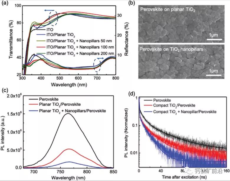
Figure 2: The effect of GLAD-derived TiO2 on the transmittance of the electrode and the performance of the perovskite film. a) UV-visible transmittance and reflectance of ITO, ITO/planar TiO2 (15 nm) and ITO/planar TiO2 (15 nm) and nanopillars of different lengths. b) SEM images of perovskite films deposited on planar TiO2 (15 nm) and planar TiO2 (15 nm) integrated nanopillar (100 nm) layer. c) Fixed PL and d) TRPL decay curves. These perovskites are manufactured on substrates that do not use or use different types of TiO2.

Figure 3: Characterization of device performance. a) Schematic diagram of the device structure. b) J-V curve of PSC based on planar TiO2 (15 nm), which does not have (w/o) or has (w/) nanopillars of different heights. c) EIS curve of PSC based on the integration of planar TiO2 (15 nm) and nanopillars (100 nm) without or without ALD TiO2 passivation. d) J-V curve of PSC based on planar TiO2 (15 nm) and planar TiO2 (15 nm) combined with nanopillars (100 nm) without ALD TiO2 passivation. e) EQE and corresponding integrated photocurrent of PSC based on ALD TiO2 passivation of planar TiO2 (15 nm) and planar nano TiO2 (15 nm) and nanopillar (100 nm) integrated PSC. f) PCE histograms of 18 PSCs, which are based on the combination of planar TiO2 (15 nm) (black) and planar TiO2 (15 nm) and nanopillars (100 nm) (red), and have ALD TiO2 passivation .

Figure 4: Study the adhesion of the perovskite film and the flexibility of the device. a) Scotch tape peeling test: a schematic diagram of the peeling test (above) and a photo of a perovskite film on a PET/ITO substrate (15×15 mm) coated with planar TiO2 or planar TiO2 with integrated nanopillars. The two photos (middle) are films prepared before the peel test. These two photos (bottom) are films that have been peeled off the transparent tape 10 times. After 200 bending cycles, SEM images of b) planar TiO2 with a bending radius of 10 mm and c) perovskite film deposited on planar TiO2 with integrated nanopillar layer. Dotted lines show cracks. Finite element simulation based on d) planar TiO2 and e) flexible perovskite film integrated with planar TiO2 and nanopillars under bending. f) J-V curve of PET/ITO-based flexible PSC based on planar TiO2 and planar TiO2 with integrated nanopillars. All devices are based on ALD TiO2 passivation. g) Normalized PCE of planar TiO2 and planar TiO2 integrated with nanopillar-based flexible devices, measured after bending cycles with a bending radius of 10 mm or 4 mm.


