 For a long time, transmission electron microscopy (TEM) has been used as the ultimate characterization technique for atomic-scale nanomaterials. In this article, the importance of using graphene in TEM is also proposed to introduce the characteristics that make it indispensable for characterizing other nanomaterials, and to study its performance and van der Waals interaction. Provides a broad overview of the importance of using TEM to study nanomaterials, and the rise of graphene as a superior substrate for studying various low-dimensional materials. This article reviews the morphology, performance and behavior of a series of nanomaterials, focusing on how graphene promotes these studies due to its unique influence and interaction on specific materials under transmission electron microscopy. This article outlines various research and characterization of a series of nanomaterials using TEM and graphene, and discusses future challenges and engineering applications.
Graphene-excellent performance as a TEM substrate
Graphene is the thinnest material with a highly crystalline morphology. The pure crystalline original graphene is also electronically "transparent" to TEM, with a resolution of up to 2.13 Å, which is the resolution obtained by many low-temperature transmission electron microscopes. This is because the 2.13Å crystal periodicity is higher than that of graphene, making it an effective "transparent" substrate. In addition, the transmission coefficient of graphene varies greatly, effectively making it transparent at a specific acceleration voltage. The thickness of a single atom of 0.34 nm hardly generates background noise. Even if the lattice is completely resolved, the signal can be easily filtered through its Fast Fourier Transform (FFT) as needed. This makes it easy to focus and study other nanomaterials on its surface, because either graphene is completely invisible at higher voltages, or its lattice can be completely filtered out of the image. Graphene is also very mechanical and elastic, which allows it to withstand the high vacuum conditions inside the TEM. In addition, it is known to be a good electrical conductor, and its electrical conductivity is six orders of magnitude higher than that of amorphous carbon, so it will not be charged from the electron beam. Comparing conventional amorphous carbon and graphene as TEM gate substrates, the thickness of graphene is one atom, while the thickness of amorphous carbon sheet can be between 3 and 20 nm. In addition, the chemical inertness of graphene makes it less reactive than amorphous carbon substrates at lower acceleration voltages. In addition, as mentioned earlier, crystalline graphene can be easily masked by Fourier filtering of the image, which is impossible for amorphous substrates. The conductive properties of graphene give it an additional advantage, that is, it has a uniform surface potential and can reduce the phase distortion of electron waves. Single-layer graphene oxide (GO) is another related material that is widely used as a substrate for microscopes. At first, when the large-area synthesis and transfer of single-layer graphene were still difficult, graphene oxide could be easily prepared or transferred to different substrates. However, despite its atomic layer thickness, its conductivity is limited, depending on the degree of oxidation. With the advent of graphene chemical vapor deposition (CVD) synthesis technology, large-area graphene can be easily synthesized and transferred as a TEM substrate, thereby alleviating the inherent limitations of the use of graphene oxide films. The availability of large-area graphene allows graphene to be easily transferred from the copper substrate to the TEM grid, thereby producing independent graphene, providing sufficient surrounding space, and having sufficient contrast to adjust the microscope and focus on the sensor. Outside the area of interest. It is worth noting that multilayer graphene (MLG) is easier to synthesize and therefore easier to obtain. However, despite its superior stability, multilayer graphene tends to be harder and more polluting than single-layer graphene. Therefore, although multilayer graphene is still much better than amorphous carbon or graphene oxide substrates, single-layer graphene is generally favored for its clean and flexible surface (Figure 1).
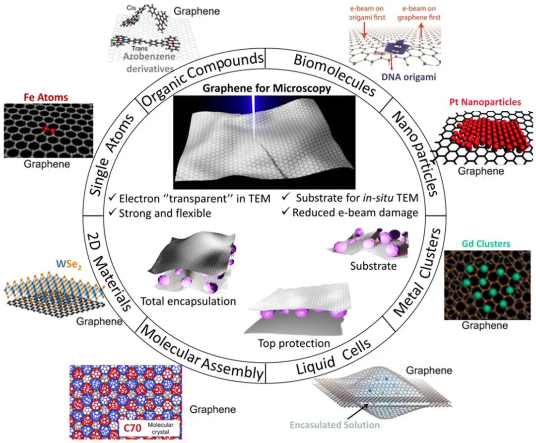
Figure 1. Schematic diagram of the advantages and different uses of graphene in transmission electron microscopy
Another type of film commonly used to image individual nanoparticles or molecules is carbon nanotubes (CNTs). The development of carbon nanotubes is earlier than graphene, so many in-situ TEM studies using carbon nanotube substrates have been carried out before then. Molecules, ions or atoms are easily confined in carbon nanotubes. Carbon nanotubes can be used as nanocontainers to study the one-dimensional properties of individual species. CNTs are strong, thermally stable, mechanically strong, and can be atomically thin, which helps to directly study molecules in real space through the walls of nanotubes. In the past 20 years, dozens of different types of nanomaterials have been wrapped on CNTs grids, and then TEM is used for research, such as molecules, nanoparticles, fullerenes, organic or biomolecules, etc. Expanding the application of carbon nanotubes beyond nanocontainers, it is also used as a container for nanoreactions. Carbon nanotubes provide an efficient platform for complex molecules, and their highly stable and robust characteristics enable it to control the encapsulated nanomaterials, and at the same time provide a real space for imaging and studying chemical reactions at the molecular level. The high mechanical strength, high thermal stability and chemical inertness of CNTs enable it to react in the tube under harsh conditions without damaging itself or participating in the reaction. However, the limited space and only one movable direction of motion in CNTs cannot provide any information about the behavior of two-dimensional molecules. In addition, limited space, harsh insertion processes and curved shapes reduce the applicability of CNTs. Graphene overcomes these factors because it provides a two-dimensional surface for the free movement of nanomaterials on the surface, while CNTs only provide one degree of freedom. In addition, nanoparticles can be easily transferred on graphene by dropping them from the solution at room temperature.
The application of graphene as a substrate in transmission electron microscopy can be broadly divided into five categories: 1) Imaging of adsorbates and light atoms themselves and their interaction with graphene. 2) Use graphene as an inert and mechanically stable substrate in in-situ experiments. 3) It is directly used as a substrate for high-resolution imaging of nanomaterials, otherwise it cannot be obtained in a stand-alone form for TEM observation. 4) As a packaging unit for imaging highly electron beam sensitive materials (such as biomolecules, organic compounds, etc.). 5) As a unique material, it can guide the research and use of electrons to create and study the mixed interface with other materials or samples, and form bundles by utilizing the existence of dangling bonds of surface carbon residues.
The purpose of this review is to systematically introduce various aspects of using graphene as a substrate for electron microscopy to promote nanomaterial research. We discussed various low-dimensional materials, understood their van der Waals interaction with graphene under the transmission electron microscope, and put forward prospects for future research.
Paper information:
Rational Component and Structure Design of Noble�\Metal Composites for Optical and Catalytic Applications
Xiaojun Zeng, Yang Zhao, Xudong Hu, Galen Dean Stucky, Martin Moskovits
Small Structures
DOI: 10.1002/sstr.202000049


