In 2014, the Hone and Wang research groups confirmed the piezoelectric electronics effect in two-dimensional MoS2 for the first time, which opened the door to the field of two-dimensional piezoelectric electronics. With the continuous development of BP, BN, TMDC and other materials, the field of two-dimensional piezoelectric electronics has gradually grown into a forest. Such as: NO2 detector with detection sensitivity as high as 1/50000000, arrayed electronic devices with spatial stress resolution as low as 500um, nano-generator with output voltage as high as 0.363 eV, etc.
Based on this, Professor Pan Caofeng of Beijing Institute of Nano Energy and Systems, Chinese Academy of Sciences and Assistant Professor Chen Ping of Guangxi University reviewed in detail the research progress of two-dimensional materials piezoelectric electronics. In order to clearly understand the branches and veins of two-dimensional material piezoelectric electronics, this paper chooses the condescending point of view of material structure-piezoelectric properties-interface regulation mechanism-flexible device application , hoping to give you an one-hit embodiment. I can see the whole forest at a glance. Firstly, based on the structure of monolayer two-dimensional materials, the structures and orientation-related piezoelectric properties of non-Centrosymmetric materials, modulated intrinsic Centrosymmetric materials and organic perovskite materials are summarized. then four methods of piezoelectric electronics testing and the principle of piezoelectric interface control are introduced. finally, the potential applications of two-dimensional piezoelectric materials in flexible optoelectronic devices, sensors and data storage are described. The challenges in practical application are further prospected.
The work is published online on InfoMat under the title Piezotronics in two-dimensional materials (DOI: 10.1002/inf2.12220).
Lets extract several parts of the article to introduce to you:
1. Two-dimensional piezoelectric material.
For materials with non-Centrosymmetric structure, when external stress is applied, the center of gravity of cations and anions deviates, resulting in piezoelectric potential at the interface between semiconductors and metals. The piezoelectric potential modulates the output current by adjusting the Schottky barrier height (SBH), which will enhance or weaken the sensitivity of the sensing equipment. Since the piezoelectric electronic effect of two-dimensional MoS2 was first confirmed in 2014, the piezoelectric properties of two-dimensional materials have been widely calculated and experimentally confirmed. We divide the reported single-layer two-dimensional materials into three categories: two-dimensional inorganic materials with non-Centrosymmetric structure, modulated intrinsic centrosymmetric materials and two-dimensional organic perovskite materials.
1.1 two-dimensional inorganic materials with non-Centrosymmetric structure.
The Reed team calculated 1173 kinds of 2D layered materials from more than 50000 kinds of inorganic crystal structures, among which the monolayer materials have intrinsic symmetry breaking, that is, there are 325 kinds of monolayer two-dimensional materials with piezoelectric and electronic effects, which are roughly divided into six categories: TMDCs and Janus TMDCs, II-VI, III-V, III-VI and Janus III-VI, IV-VI and VmurV (figure 2).
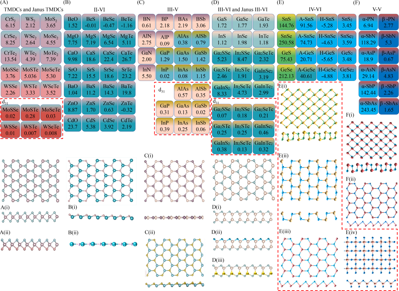
Figure 1.
Piezoelectric coefficient and Crystal structure of six kinds of monolayer two-dimensional Materials.
1.2 Intrinsic Centrosymmetric Materials modulated.
Through interfacial interaction, adsorption of atoms and induction of specific defects, the two-dimensional material with Centrosymmetric structure is modulated to become a two-dimensional material with piezoelectric properties.
1.3 two-dimensional organic-inorganic hybrid perovskite.
With the maturity of perovskite preparation technology, two-dimensional organic-inorganic hybrid perovskite has been developed into a new type of piezoelectric material. At present, the non-centrally symmetrical structure of two-dimensional organic-inorganic hybrid perovskite has been confirmed by PFM and second harmonic, and the piezoelectric electronic effect of organic-inorganic hybrid perovskite has been gradually developed.
two。. Piezoelectric Electronics Regulation Mechanism of two-dimensional Materials.
At present, there are four kinds of piezoelectric electronic effect detection methods: bending and release of flexible devices, atomic force microscope (AFM), PFM, scanning probe microscope (SPM). The piezoelectric regulation mechanism is to increase or decrease the height of the Schottky barrier through the piezoelectric potential caused by the accumulated charge at the interface, resulting in the increase or decrease of the depletion region, resulting in the decrease or increase of the output current and the change of induction sensitivity.
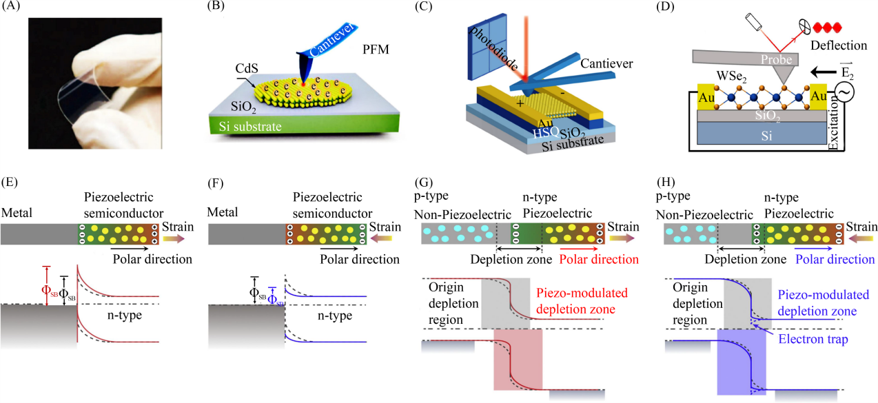
Figure 2.
Test method and Micro-mechanism of piezoelectric Electronics for two-dimensional material piezoelectric Devices
3. Potential applications of two-dimensional materials in piezoelectric electronics.
At present, potential applications based on two-dimensional piezoelectric / piezoelectric optoelectronic effects are gradually developed, including various sensors, such as stress, gas, micro-vibration, light detection, humidity, nano-generator, piezoelectric catalysis, information storage and other applications. Take the nano-generator as an example.
Based on the atomic layer thickness and excellent mechanical and piezoelectric properties of two-dimensional materials, two-dimensional piezoelectric electronics has made great breakthroughs in energy collection and self-driving systems.By applying tensile or compressive strain, a piezoelectric potential is generated at the interface between the two-dimensional material and the metal electrode, and the electrons and holes in the material are attracted by the opposite polarity of the piezoelectric potential, resulting in an electric current. When alternating strain is applied, AC output current and voltage are generated. So mechanical energy is converted into electricity, that is, nano-generators. Hone and Wang research team discovered the nano-generator based on odd-layer MoS2 for the first time, and achieved 5.08% electromechanical energy conversion efficiency of single-layer MoS2 nano-generator. The piezoelectric output of the single-layer MoS2 nano-generator is related to the crystal orientation, and the piezoelectric coefficients in the zigzag and armchair directions are different, which leads to the difference of the piezoelectric output. at the same time, the series nano-generator increases the output current, and the parallel nano-generator increases the output voltage. Subsequently, the nano-generators of two-dimensional materials have received extensive attention, based on MoSe2, α-In2Se3, BP, MoS2 hollow spheres, BN, ZnO, double-layer WSe2, porous MoS2 and other two-dimensional nano-generators have been reported. The realization of double-layer WSe2 nano-generator shows that the stacking orientation of even-layer TMDCs determines the symmetry and piezoelectric properties of the material (figure 4 Dmurf). Another influential work is the single-layer porous MoS2 nano-generator designed by Raddovic research group. Two-dimensional MoS2 with porous structure separates two liquids with different concentrations, thus forming a concentration gradient, which leads to the spontaneous penetration of ions through the porous structure. At the same time, due to the specific surface charge around the porous structure, the ions passing through will be selected according to the charge polarity, thus generating a net osmotic current. This type of nano-generator successfully pumped the MoS2 transistor to form a self-driving system. These groundbreaking work have laid the foundation for the practical application of nano-generators, and integration and wearability will become the topic of development in the future.
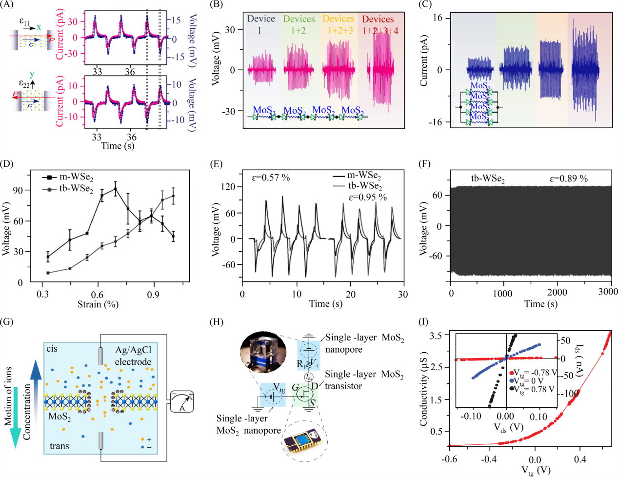
Figure 3.
Nano-generator based on two-dimensional material.
4. Summary and prospect.
Two-dimensional material piezoelectric electronics can significantly improve the sensitivity of optoelectronic components, combined with the good mechanical properties of two-dimensional materials, and has potential application value in sensing, display, power generation, information storage and other application fields. However, there are still many key scientific and technical problems to be solved in the piezoelectric electronics of two-dimensional materials. First, at present, the research on piezoelectric electronics of two-dimensional materials is in the stage of preliminary discovery of phenomena, and horizontal and vertical qualitative and quantitative research is urgently needed. Second, in the research process of piezoelectric electronics of two-dimensional materials, in addition to the piezoelectric potential caused by strain, the energy band structure of two-dimensional materials is also very sensitive to stress engineering, which will also affect the transport properties of electrons. Third, the effects of different kinds of defects and defect concentrations in two-dimensional materials on carrier transport and separation under stress need to be calculated and verified by experiments. Fourth, for further practical application, it is necessary to develop array devices without serial interference. Fifth, the growth of two-dimensional materials and piezoelectric electronics testing methods should be further developed.
Introduction to the author.
Pan Caofeng, Professor / doctoral Supervisor, Beijing Institute of Nano Energy and Systems, Chinese Academy of Sciences. Mainly engaged in low-dimensional piezoelectric semiconductor piezoelectric (optical) electronics effects, new micro-nano optoelectronic functional devices, tactile electronics and intelligent robot research. Based on low-dimensional piezoelectric semiconductors, starting from material design and controllable preparation, the modulation mechanism of piezoelectric (optoelectronic) electronics effect on the performance of piezoelectric (optoelectronic) semiconductor devices is explored. Important progress has been made in the fields of ultra-high resolution stress sensing and imaging, high performance sensors, biological interaction and control. In Chem. Rev. 、 Nat. Photon. 、 Nat. Comm. 、 Adv. Mater. 、 Adv. Energy Mater. 、 Angew. Chem. Int. More than 190 SCI papers have been published in Edit., Nano Energy, ACS Nano and other journals, with more than 8200 citations. He is currently Deputy Editor-in-Chief of Materials Science of Science Bulletin Journal and Deputy Editor of Nanotechnology Optoelectronic Devices. Chen Ping, Assistant Professor / Master Supervisor, College of physical Science and Engineering, Guangxi University. Mainly engaged in two-dimensional material synthesis, optical, electrical, magnetic and other mechanism regulation of micro-nano devices, and rare earth ion single particle fluorescence modulation and so on. More than 20 SCI papers (12 first / newsletter authors) have been published and cited more than 300 times.
This information is from the Internet for academic exchange only. if there is any infringement, please contact us to delete it immediately.


