已传文件:photo/1655705068.png
The characterization equipment of Beike Nano Characterization Laboratory is as follows:
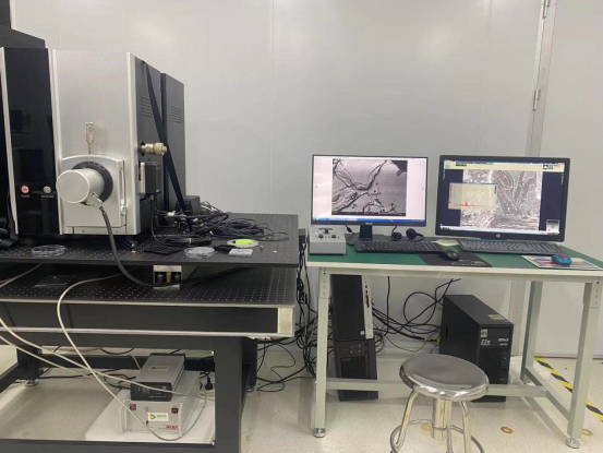
Electron microscope + energy spectrum SEM + EDS:
It is used to characterize the morphology and microdomain composition of materials above 100nm.
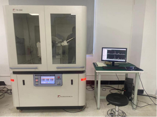
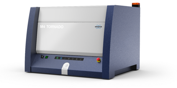
Polycrystalline Powder Diffraction XRD:
For physical property testing of materials.
AFM atomic force microscope:
It is used to test the morphology of materials below 100nm, quantum dots, nanosheets, etc.
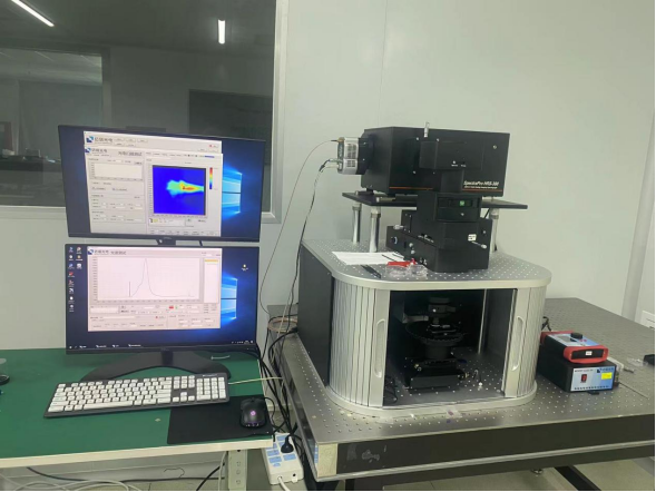
Micro area Raman+PL, Mapping equipment:
532nm laser, can perform mapping scanning in the maximum range of 100*100um.
PL spectral range: 550nm~1000nm.
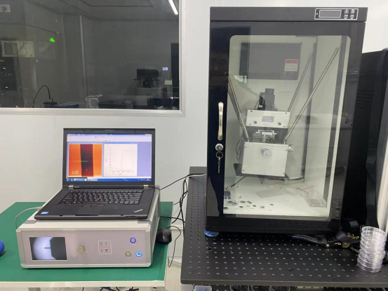
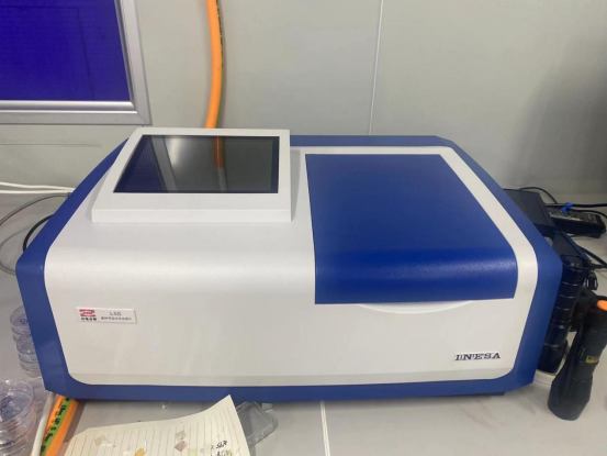
UV-VIS absorption spectrum:
The spectral range is 200nm~1100nm, which is used to test the absorption characteristics of nanosheets, quantum dots and other materials in the visible and near-infrared range.
X-ray fluorescence spectrometer XRF:
The test is similar to EDS and allows rapid material composition analysis in atmospheric environments.
Microspot spectral test:
Using a microscope to focus, it can test the absorption characteristics of 4um micro-area, and the test range is 400~1700nm.
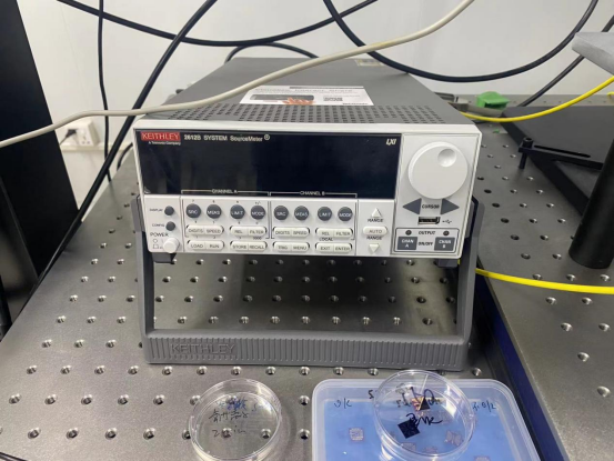
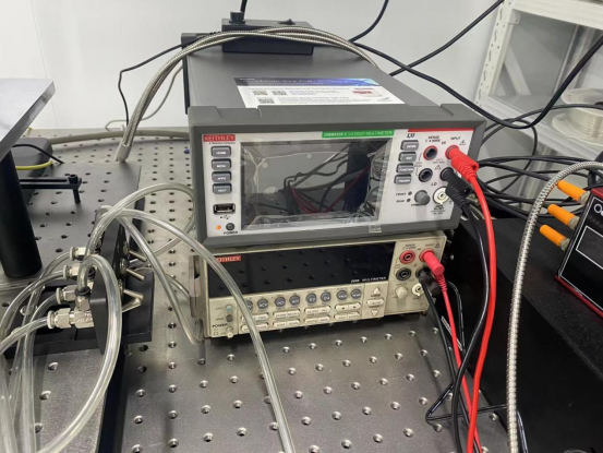
Probe station photoelectric and electrical testing:
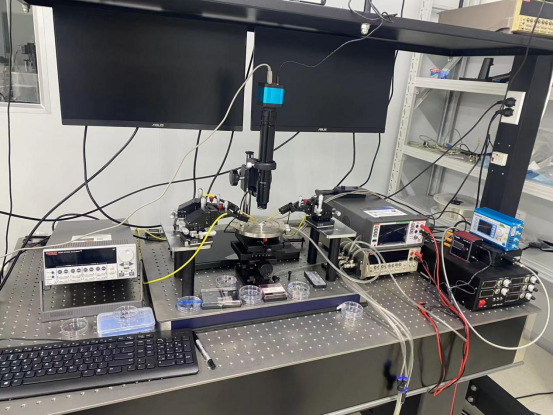
Equipped with a variety of wavelength lasers, it is used to test the photoelectric response of materials to different wavelengths.
Laser wavelength: 405nm, 532nm, 633nm, 808nm, 980nm,
1064nm, 1550nm, 1920nm.
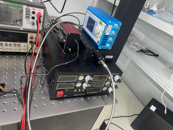
Electrical test configuration: Keithley 2612B, Keithley 2000, Keithley 2010, Keithley DMM 6500, etc.
A variety of source meters and precision test equipment.
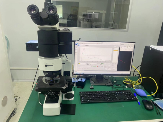
Multiple metallographic microscopes:
For rapid sorting of material morphology.
More analytical testing equipment is being purchased externally or built by itself as the scope of material research and development expands.
In addition, North Konami cooperates with a number of advanced technology companies and top university research groups to conduct more high-end tests as needed.


