�Ѵ��ļ���photo/201986145455715.png
The use of computer simulation based full electromagnetic field numerical simulation is one of the important research methods for studying optoelectronic devices. In particular, with the rapid development of optoelectronic device configuration toward ultra-small size and on-chip integration, the use of traditional linear optical and thin film optical analysis methods and approximate theoretical modeling has been unable to provide a comprehensive analysis of the device��s operating characteristics. In more complex systems, researchers often need to combine the excitation and transport of materials such as photogenerated carriers, near-far field expansion calculations, and the physics characteristics of the luminescent materials to comprehensively analyze the working process of the device. At this time, the use of multi-physics coupled one-stop device simulation can greatly reduce the theoretical analysis difficulty of the researchers, and provide more comprehensive data support for experimental observations and theoretical models, making our research papers more complete and vivid. .
At present, the mainstream full electromagnetic field simulation technology can be roughly divided into frequency domain finite element simulation represented by COMSOL and time domain finite difference simulation represented by FDTD technology. Both technical means can deal with various complex micro-nano device simulation problems, and show their unique technical advantages in some special scenarios.
In this article, we have compiled and analyzed some classic cases of micro-nano-optical devices using full-electromagnetic field numerical simulation in recent years, so that we can have a better understanding of this research method.
Realizing the structural design and performance optimization of the device has always been one of the important application scenarios using device analog technology, especially in the fields of photoelectric conversion devices, photonic crystals, and micro-nano antennas. This type of device design problem often involves multi-physics coupling, large parameter space, etc., and is particularly suitable for processing using computer-aided design (CAD).
Taking the design of a solar cell with a micro-nano configuration as an example, we generally use the Maxwell equation directly to obtain an accurate electromagnetic field distribution in an irregular, ultra-thin or resonant-supporting device structure, combined with the energy band of the semiconductor material/ The energy level characteristics calculate the photogenerated carrier excitation rate inside the device. Then, the excitation information is imported into the finite element analysis solver to calculate the carrier and then specify the operating field under the operating voltage, and thereby establish the electrical output characteristics of the device. Device simulation can help researchers optimize the optical absorption characteristics of solar cells and the ability to collect photogenerated carriers.
For example, Professor Sargent of the University of Toronto, Canada, used device optical simulation technology to carefully design the surface structure of quantum dot thin film solar cells, improve their refractive mode of incident light, and improve the optical absorption capacity of thin films (Nano Letters | 10.1021/acs.nanolett. 6b05241).
Researchers at Xijiang University in South Korea, with the aid of optical simulation of the device, combine photonic crystals with device electrodes and the optical and electrical properties of perovskite cells (Nano Energy| 10.1016/j.nanoen.2018.11.050).
The well-designed device shape that supports the resonant mode also allows limited incident light to converge inside the device, allowing even a single nanowire to achieve device performance beyond traditional theoretical limits (Nature photonics| 10.1038/nphoton.2013.32).
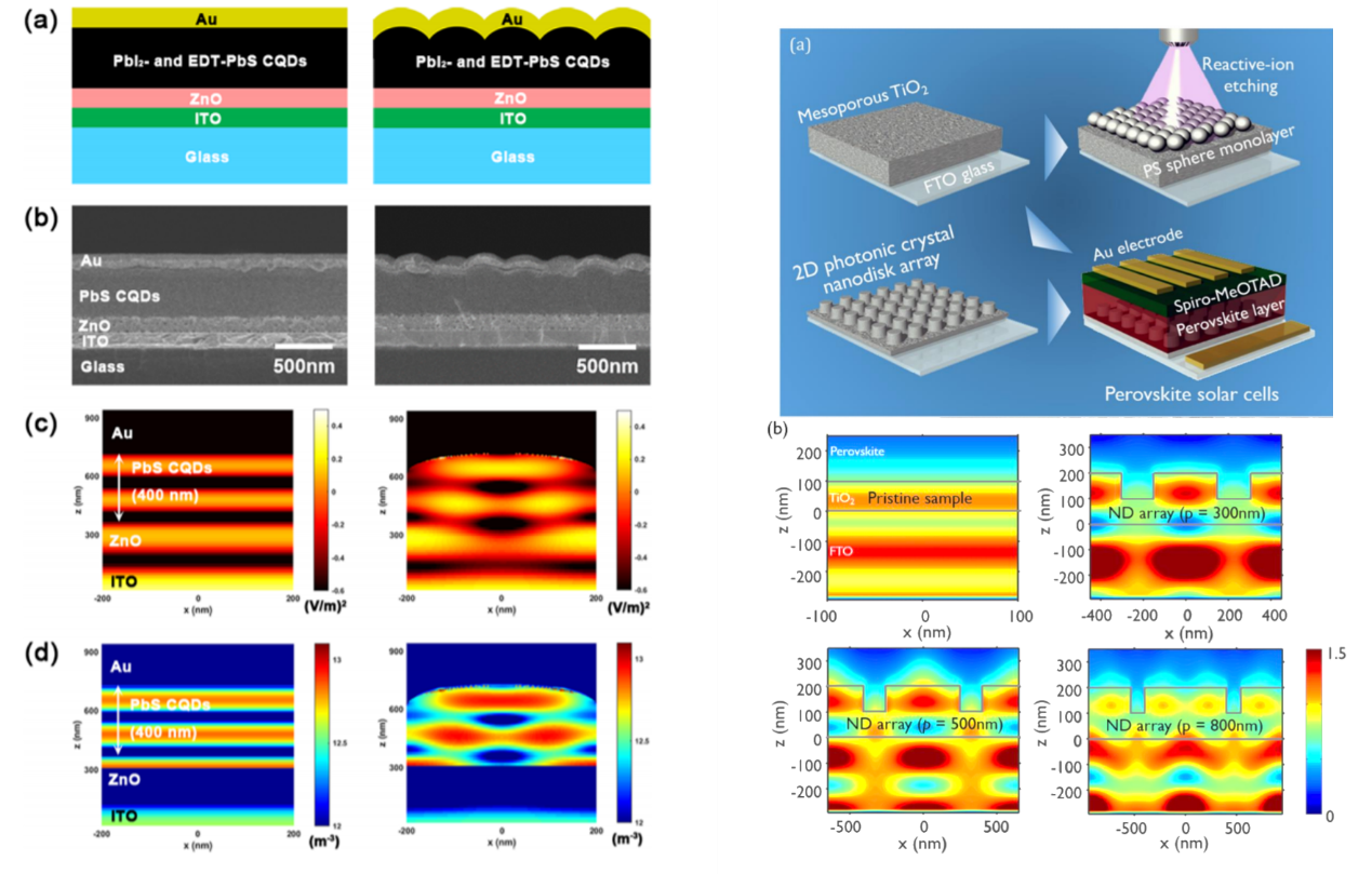
Figure 1 Left: Design of surface optical structure for quantum thin film cells by FDTD numerical simulation (Nano Letters | 10.1021/acs.nanolett.6b05241); Right: Design 2D photonic crystal electrode layer for perovskite solar cells by full electromagnetic field numerical simulation ( Nano Energy|10.1016/j.nanoen.2018.11.050).
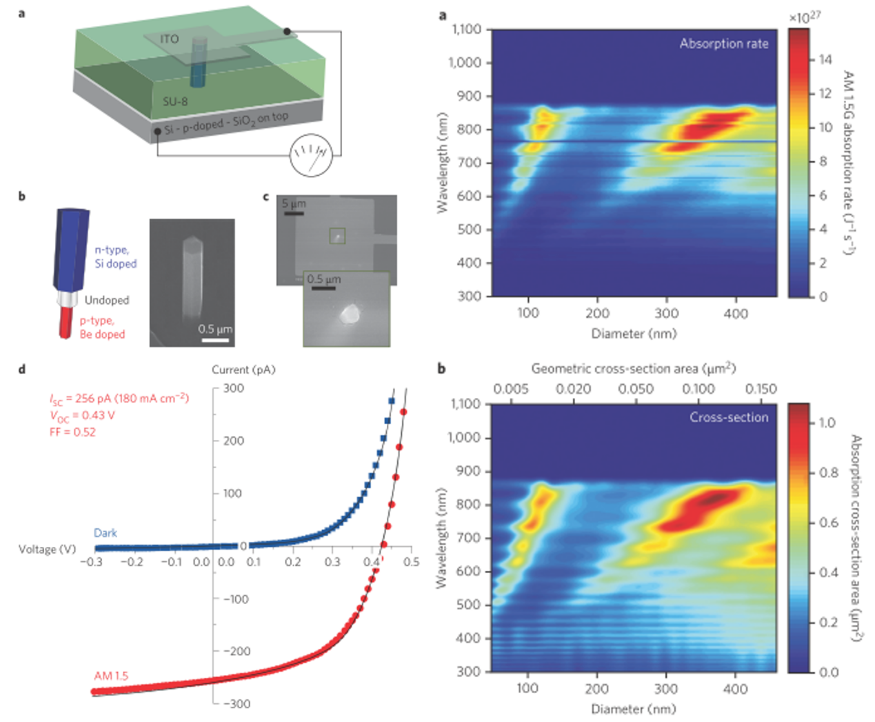
Figure 2 is based on a single nanowire GaAs solar cell. Obtained device conversion efficiencies beyond the Shockley�CQueisser limit through device-based optical design (Nature Photonics | 10.1038/NPHOTON.2013.32)
In the field of traditional micro/nano optics design, due to the advanced all-electromagnetic field simulation technology, researchers can more easily handle some more complex and more demanding optical systems to provide various specific optical properties. .
For example, researchers at Fudan University used a numerical simulation of electromagnetic fields to provide a more comprehensive detail analysis of their plasma super-surface design (Nanoscale| 10.1039/C8NR02088D). This super-faceted surface can effectively convert the Gaussian speed of light into a vortex, and its theoretical conversion efficiency can exceed 40%, and has good broadband characteristics.
The following research results from the University of Technology, Sydney, Australia (Nature Communication | 10.1038/s41467-018-05117-4) are also developed using a numerical simulation technique to develop a device for quantum electrodynamics (QED) experiments. The high performance hexagonal boron nitride photonic crystal resonator has a resonance quality factor of over 2000 and exhibits properties that are insensitive to processing.
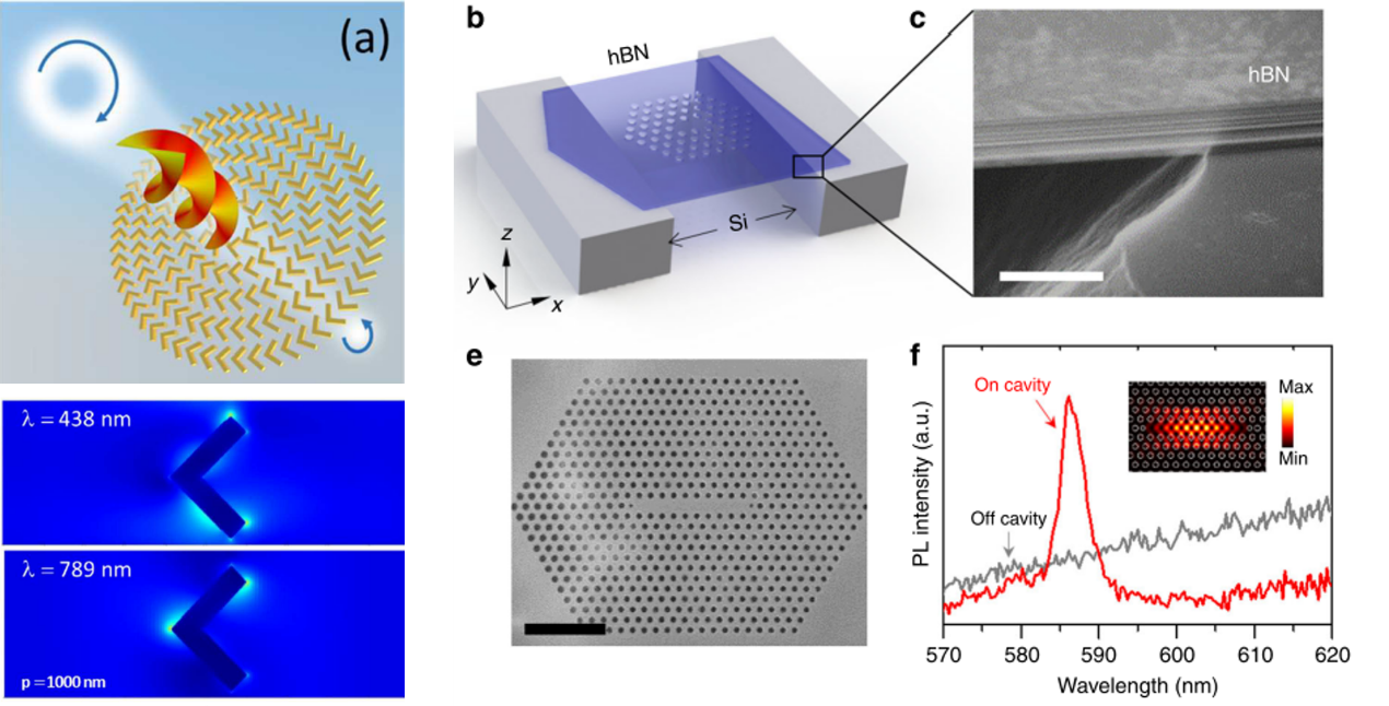
Figure 3 Left: Using the device optical analog design to design the surface details (Nanoscale| 10.1039/C8NR02088D); Right: Using the device optical simulation to design a high performance hexagonal boron nitride photonic crystal resonator (Nature Communication | 10.1038/s41467-018-05117- 4)
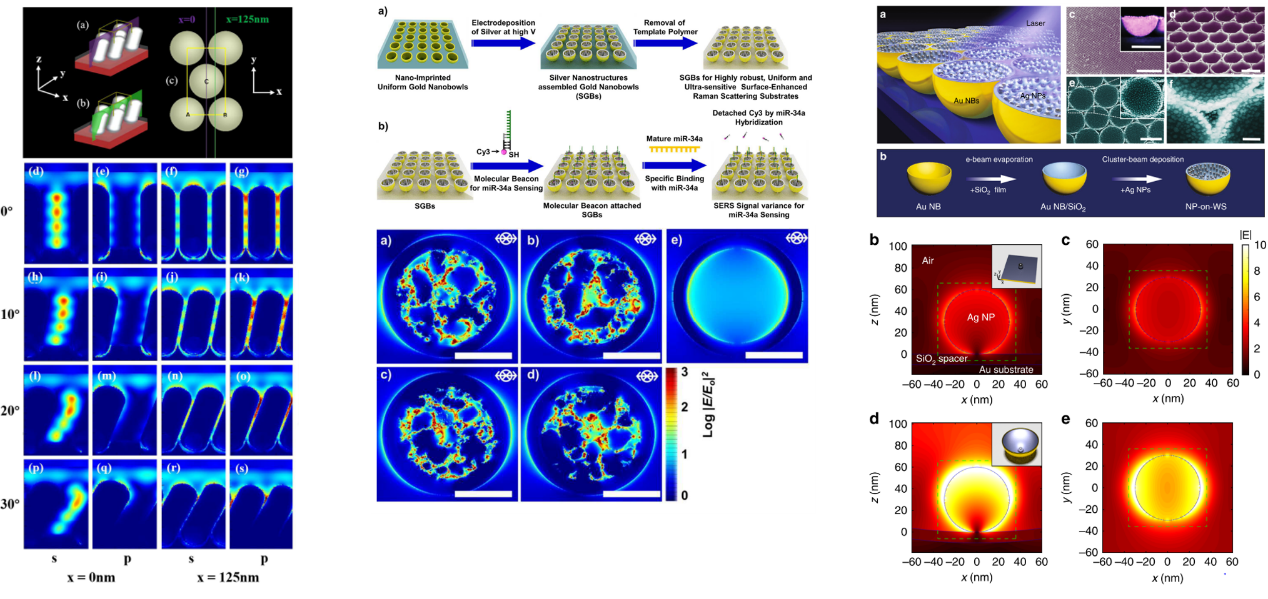
Figure 4 uses the full electromagnetic field numerical simulation to assist in the design of metal nanostructures in SERS. Left: Nanoscale |10.1039/C8NR01198, Medium: Nanoscale | 10.1039/C7NR08066B, Right: Nature. Communication |10.1038/s41467-018-07869-5
In the field of surface plasmon resonance, designing high-performance surface-enhanced Raman scattering (SERS) is a hot trend in recent years and an important detection technology in the field of biochemistry. The full electromagnetic field simulation can accurately calculate the electromagnetic field distribution characteristics near the metal nanoparticles and calculate the optimized SERS efficiency.
Scholars from Jilin University (Nanoscale |10.1039/C8NR01198B), Yonsei University (Nanoscale |10.1039/C7NR08066B) and the University of Birmingham (Nature.Communication | 10.1038/s41467-018-07869-5) have used this method to study different methods. The effect of nanostructures on the efficiency of SERS devices.
In addition to device design, another important application of device simulation is to aid in the interpretation of experimental phenomena and comparative proof theory analysis. In studying the luminescence properties and experimental spectra of GaN nanopillars, researchers at the Max Planck Institute for Light Science in Germany used device numerical simulations to calculate the resonant optical modes in nanopillars to explain the multimodal properties of their characterization spectra (Nano Letters| 10.1021/acs.nanolett.6b00484).
In addition, when studying superlattice nanowire lasers, researchers at the University of Tokyo (Nature Photonics| 10.1038/NPHOTON.2015.111) Norwegian University of Science and Technology (Nano Letters | 10.1021/acs.nanolett.7b05015) also chose to use device numerical simulation. The technology assists in measuring the laser threshold, coupling coefficient and far-field interference patterns of the device, and obtains a good agreement with the experimental observations.
In the field of near-field optical effects research, the rational use of electromagnetic field numerical simulation can also help us study the basic physical properties of the system. The near-field effect converges the electromagnetic field to accelerate the spontaneous emission rate of the excitation element, that is, the Purcell effect makes a kind of representative near-field optical effect.
Researchers from Rice University in the United States used this property to obtain the hot electron fluorescence signal of the gold nano-stick (ACS Nano | 10.1021/acsnano.7b07402), and researchers at Royal Institute of Technology in Sweden used this physical phenomenon to enhance spectral up-conversion. The fluorescence efficiency is more than 400 times (Nanoscale | 10.1039/C8NR08653B, and the University of Colorado scholars have used it to enhance the radiation efficiency of dark exciton (Nature Nanotechnology | 10.1038/s41565-017-0003-0) .
The above three research results are inseparable from the theoretical value of Purcell factor calculated by optical simulation of the device, which is an important reference for experimental design and theoretical argumentation.
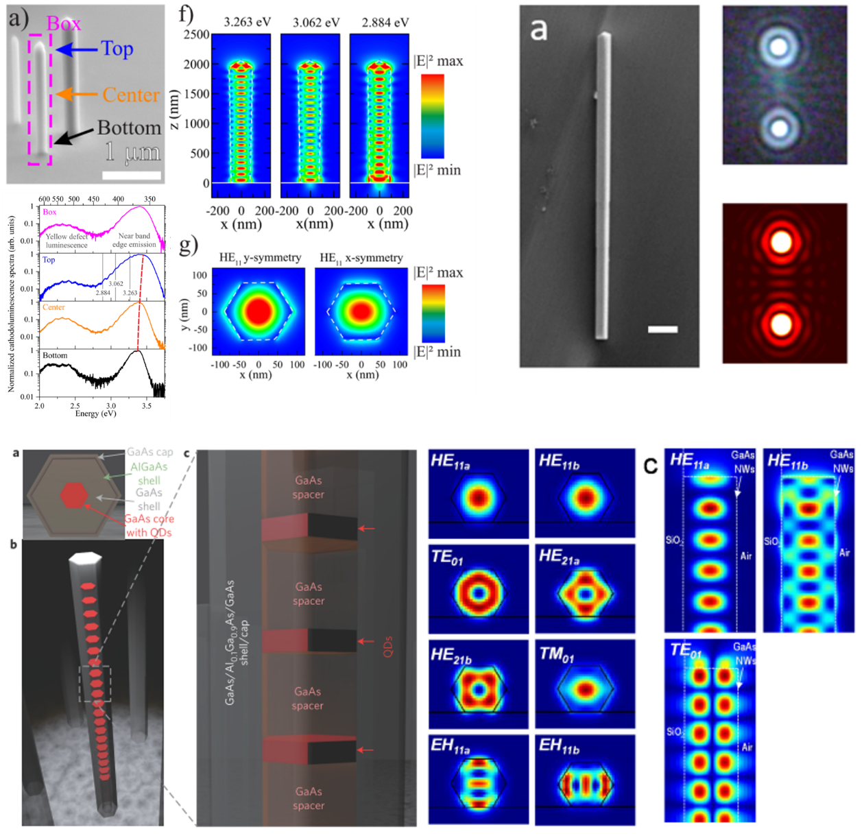
Figure 5 Top left: Optical resonance inside the GaN nano-pillar leads to multi-peak characteristics of its spectrum (Nano Letters | 10.1021/acs.nanolett.6b00484); Top right: Far-field interference pattern of InGaAs superlattice nanowires (Nano Letters | 10.1021/acs.nanolett.7b05015);Bottom: Resonance mode and laser excitation analysis of GaAs superlattice nanowires (Nature Photonics| 10.1038/NPHOTON.2015.111)
In fact, the use of time domain numerical simulation represented by FDTD has extremely unique advantages in calculating the Purcell factor and local photon density. Due to the time domain full electromagnetic field calculation characteristics of FDTD, it can naturally simulate the interaction between the radiated electromagnetic field and the radiation source. Therefore, we can use the dipole in the device structure and in the general medium background in the FDTD simulation environment. The ratio of the radiant energy directly obtains the numerical solution of the local Purcell factor.
Theoretical analysis shows that (Optics Letter | 10.1364/OL.37.002880), even in the dissipative systems that traditional classical theoretical models are difficult to accurately process, such as absorbing materials, open boundaries, etc., the simulation results of FDTD still have super high self-consistent Sex and accuracy provide highly reliable reference values for theoretical and experimental research.
From the above examples, we can see that the use of full electromagnetic field numerical simulation has become one of the important theoretical means of micro-nano optoelectronic device design and research. The full use of simulation technology can greatly improve the theoretical level and completeness of our article, and make the research quality and the standard of the paper to a higher level.
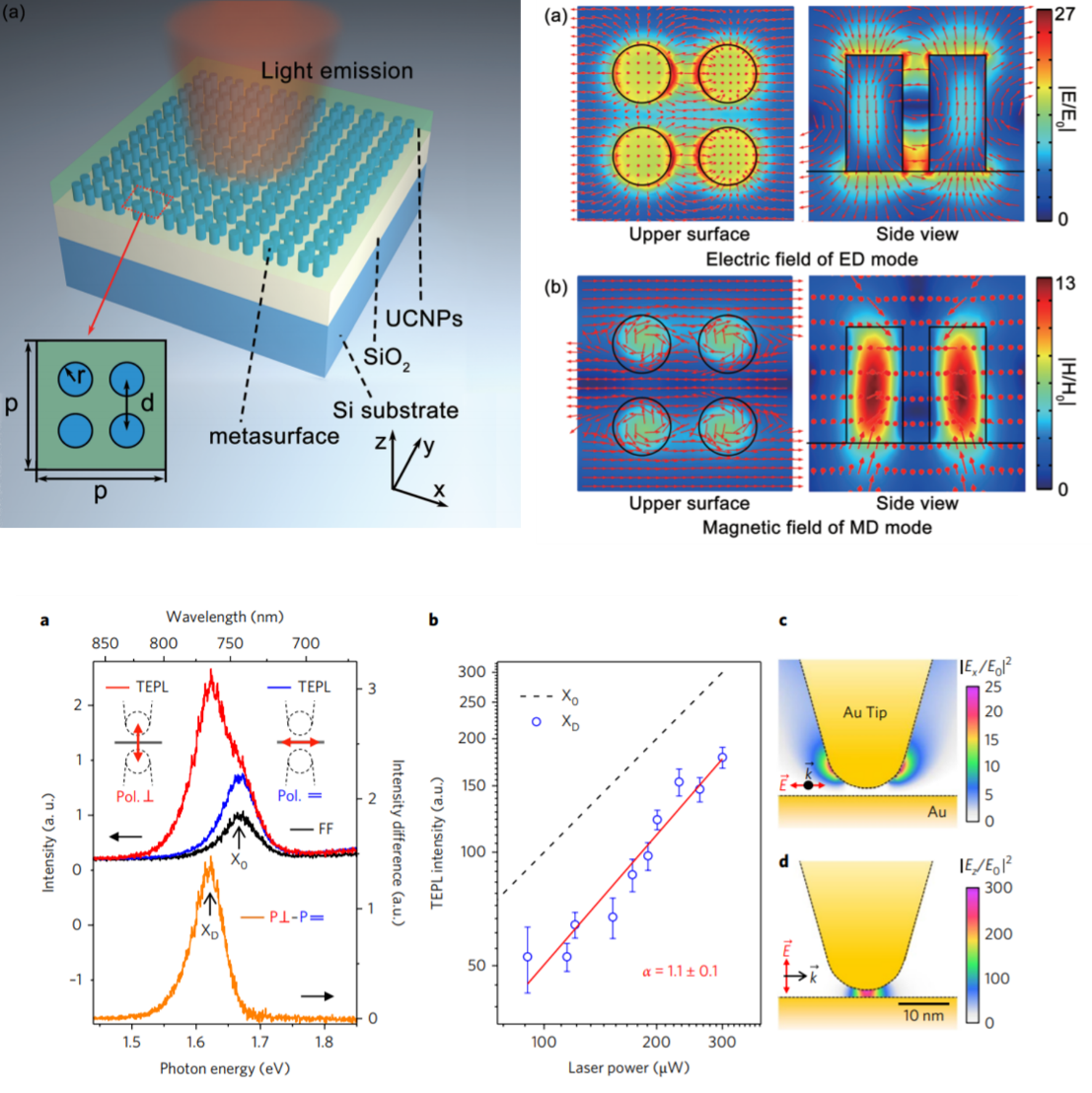
Figure 6: Purcell effect enhancement spectral up-conversion efficiency using the all-media super-superior surface (Nanoscale| 10.1039/C8NR08653B); Bottom: Enhancement of dark-exciton radiation using the metal-tip Purcell effect (Nature Nanotechnology | 10.1038/s41565-017 -0003-0)
��ԴSource��
http://www.cailiaoniu.com
http://www.nanoer.net


