
Research Background
Memory computing architecture is considered one of the most promising technologies beyond traditional complementary metal oxide semiconductor (CMOS) technology. Traditional von Neumann computing architectures face the huge challenge of providing higher performance and lower power consumption due to bottlenecks between logic and memory modules. Memory computing devices, such as artificial synaptic devices and non-volatile device-based ternary content addressable memory (TCAM), have become potential candidates for electronics in the future, and have caused great potential in recent years. Research concerns. So far, many non-volatile devices have been implemented in experiments, including resistance random access memory (RRAM), phase change memory (PCM), ferroelectric field effect transistor (FeFET), and magnetic random access memory (MRAM). ). Due to the diversity of energy band structures, 2D van der Waals heterojunctions show great potential in multifunctional devices including memories and logic. In addition, artificial synaptic devices based on 2D materials have also been shown to have the potential of multifunctional artificial neural networks (ANN) and neuromorphic computing. However, the previously demonstrated devices related to non-volatile multi-valued logic operations and multi-language synaptic operations still lack diversity and versatility. New electronic devices can be explored based on emerging 2D materials and their heterojunctions, providing new ideas for the development of logic memory devices.
Achievements
In view of this, recently, a team of Professor Wu Yanqing of Huazhong University of Science and Technology reported on a 2D van der Waals heterojunction based on direct band gap materials black phosphorus (BP) and thorium disulfide (ReS2) for nonvolatile ternary logic operations. The ultra-thin black phosphorus oxide layer is used as a charge trapping and inter-band tunneling layer. The artificial electronic synapse based on this heterojunction has been proven to achieve trilingual synaptic response by changing the input base voltage. In addition, using handwritten digital data, artificial neural network simulations based on electronic synaptic arrays can achieve a high recognition accuracy of 91.3%. This work provides a way to implement multi-functional non-volatile logic logic storage applications based on novel 2D heterojunctions. The article was published under the title "Reconfigurable Logic-in-Memory and Multilingual Artificial Synapses Based on 2D Heterostructures" Journal Advanced Functional Materials
Graphic guide
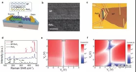
Figure 1. Van der Waals heterojunction and device characterization. (A) Schematic diagram of BP / ReS2 heterojunction device and schematic diagram of the lattice cross section of the junction region interface. The drain is deposited on the BP layer, and the source is deposited on the ReS2 layer. (B) A cross-section high-resolution TEM image of the BP / ReS2 interface, with a POx layer of approximately 4 nm observed. (C) Optical micrograph of the device. (D) Raman spectra of BP, BP / ReS2 overlap and ReS2 region. (E, f) Current of BP / ReS2 heterojunction with different Vd and Vg bias at 300 K and 4.3 K.
Figure 1a shows a schematic diagram of a BP / ReS2 heterojunction device. The mechanically peeled BP and ReS2 wafers are transferred to a 25 nm HfO2 covered silicon substrate, and the source / drain electrodes are formed by EBL evaporation of 20/40 nm Ni / Au. . The high-resolution TEM of the cross section of the BP / ReS2 heterojunction is shown in Figure 1b, where a highly crystalline layered lattice of BP and ReS2 can be seen, with a 4 nm POx layer between BP and ReS2. Figure 1c shows the optical microscopy image of the device. The thickness of BP and ReS2 was determined by AFM to be about 10 and 7 nm, respectively. The Raman spectra of the three positions of the BP / ReS2 heterojunction (including the BP region, the ReS2 region, and the junction region) are shown in Figure 1d. The Raman spectrum of the junction region is the superposition of characteristic peaks of the two materials. Figures 1e and f show the imaging of the drain current Id as a function of the drain and gate voltages at 300 K and 4.3 K for the BP / ReS2 heterojunction. A drain voltage of -3 to 3 V is applied to the BP terminal, and the ReS2 source terminal is always grounded. Due to different band alignment conditions under various voltage biases, the drain current exhibits non-monotonic dependence and has continuous adjustability at Vg of -4 to 4 V and Vd of -3 to 3 V This is even more pronounced at 4.3 K. These changes can be attributed to the band arrangement shift, in which the heterojunction junction region changes from a ReS2-dominated n-p junction to a BP-dominated n-p junction and n-n junction.
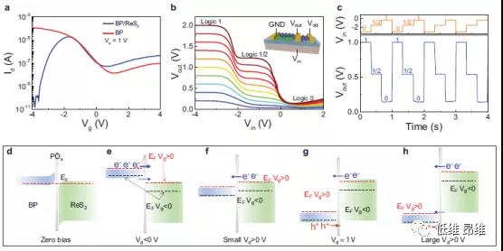
Figure 2. Ternary logic circuit. (A) Transfer characteristics of BP FET and BP / ReS2 heterojunction FET at Vd = 1 V. (B) When Vdd is 0.1 to 2 V, the change of Vout with respect to Vin of the ternary inverter of the BP / ReS2 heterojunction series BP FET. Inset: Circuit diagram of a ternary inverter. (C) The ternary input waveform and ternary logic output waveform at 1 Hz of the inverter. (D) Band diagram of heterojunction under thermal equilibrium at zero bias. (E-h) Band diagram of heterojunction with negative Vd bias and positive Vd bias.
Compared with traditional binary logic, multi-valued logic devices can achieve higher data density with less disk space. By using BP / ReS2 heterojunction FET and BP FET in series, a ternary logic circuit based on 2D materials is realized. Figure 2a shows the individual transfer characteristics of a BP FET and a BP / ReS2 heterojunction FET with a drain voltage of 1 V. The negative transconductance region of the heterojunction originates from the inter-band tunneling mechanism, in which the drain bias bends the energy band of BP downward to form a high tunneling efficiency region. The main current changes from n-type transport of ReS2 to n-type hole tunneling through the heterojunction. It shows a downward trend with increasing gate bias. Outside the negative transconductance region, the gate bias further increases. Large, due to the strong n�Cn junction, the current will rise again. The ternary inverter of Vout versus Vin (Vdd is 0.2 to 2 V) is plotted in Figure 2b. The output characteristics show three different logic state regions, including the "logic 1" of the input voltage Vin <-2 V, 2 V 0 V ��logic 0��. The additional intermediate logic (logic 1/2) comes from the region with strong interband tunneling, where BP FET and BP The / ReS2 heterojunction FET has almost the same current trend at -2 V

Figure 3. Nonvolatile ternary logic circuit. (A) Schematic diagram of downloading energy bands for the capture and decapture processes of the carrier under negative Vg bias and positive Vg bias conditions. (B) When Vdd = 1 V, the typical double-sweep voltage transfer characteristics of a ternary logic inverter. (C) Under different Vin pulse widths, with a fixed Vin pulse amplitude of �� 4 V and Vin_base = -1.8 V, the output is switched from logic 1/2 to logic 1. (D) Under different Vin pulse widths with Vin_base = 0.3 V, the output switches between logic 0 and logic 1/2.
BP naturally oxidizes to form a charge-trapping layer on the surface, which appears as a charge-retaining layer (Figure 3a). The voltage transfer curve of the ternary logic inverter also shows obvious hysteresis under the dual voltage sweep (Figure 3b). It can be seen that two separate output states can be obtained according to the voltage sweep direction, at Vin = -1.8 "1/2" and "1" are displayed at V, and "0" and "1/2" are displayed at Vin = 0.3 V. Under the condition of fixed Vin_base = -1.8 V, the two-level output of "1/2" and "1" can be better observed through the output characteristics of the Vin pulse (Figure 3c). When the pulse width is reduced from 50 ms to 1 ms, "Logic 1" shows a small change, but the output voltage of "Logic 1/2" increases accordingly. Similarly, it is also possible to switch the two-level output of "0" and "1/2" by the Vin pulse when Vin_base = 0.3 V is fixed. The pulse width decreases and increases (Figure 3d). The results of the pulse switching show that the non-volatile ternary logic inverter can work under various input conditions.

Figure 4. Artificial trilingual synapses based on the BP / ReS2 heterojunction. (A) Schematic representation of biological and artificial synapses. (B) For three different Vg_base conditions of �C2, 0, and 2 V, a 4 V input pulse (10 ms) PSC response at the input. (C) The direction dependence of the drain current measurement under different Vg and Vd. Three different Vg conditions showed a trend of change, corresponding to 1-3 points in (b). (D) With Vd = 1 V at 300 K, the synaptic weight of a 4 V input pulse (10 ms) varies with different Vg_base. (E) With Vd = 1 V and Vg_base = 0 V at 300 K, the synaptic weight of the 4 V input pulse varies with different pulse widths. (F) Using 50 enhanced (4 V, 100 ��s) and suppressed (-4 V, 10 ��s) presynaptic inputs with Vd = 0.5 V, long-term enhancement and suppression of synaptic heterojunctions. (G) A schematic diagram of a three-layer (one hidden layer) neural network. (H) Recognition accuracy of handwritten digital images with experimental and ideal values.
Artificial synapses can be used in artificial neural networks (ANN) and neuromorphic computing, which has huge application potential for low-power next-generation computing architectures. Figure 4a shows a schematic diagram of biological and artificial electronic synapses, with the gate terminal as the pre-synaptic input and the source terminal as the post-synaptic output. Figure 4b shows the synaptic behavior of a 4 Vg pulse amplitude under three electrostatic Vg bias conditions. By adjusting the bias voltage Vg (2, 0, -2 V) of the base with a fixed Vd = 1 V, the post-synaptic current (PSC) exhibits long-term excitation and long-term suppression response. The drain currents are plotted as Vd and double-sweep Vg, corresponding to different synaptic behaviors as shown in Figure 4c. As mentioned earlier, a positive input pulse will inject electrons into the POx layer, causing PSC to increase when Vg_base = 0 V and decrease PSC when Vg_base = + 2 / -2 V. As shown in the device��s synaptic behavior dependence on Vg_base in Figure 4d, when the presynaptic input base voltage is -3 to 3 V, the three regions change from suppression to excitation, and then back to the suppression response, showing Speech response characteristics. At the same time, under the same 4 V pulse amplitude of Vd = 1 V, the synaptic weight can be adjusted. The unique tunability of the trilingual response is derived from the reverse bipolarity of the BP / ReS2 heterojunction device, and it can also be extended to other TMD materials.
Figure 4e shows the relationship between the weight change of excitatory PSCs with an amplitude of 4 V and a base value of 0 V and presynaptic input pulses. As the presynaptic input pulse width increased from 1 ��s to 100 ms, as more and more carriers were captured into the POx capture layer, the change in synaptic weight showed a monotonic change from 5% to more than ��104% Increasing the trend has a stronger impact on Fermi level movement. The largest change in long-term synaptic weights reached 23300%, exceeding the previously reported results. Figure 4f shows the PSC generated by alternately inputting 50 positive (4 V, 100 ��s) and 50 negative (-4 V, 10 ��s) gate voltage pulses, showing long-term enhancement (LTP) to biological synapses ) And long-term suppression (LTD) repeatable and stable response. Figure 4g shows a schematic diagram of a neural network for handwritten digits, which contains 784 input neurons, 300 hidden neurons and 10 output neurons for 28 �� 28 input pixels and 10 output classifications. The non-volatile heterojunction device is used as the weight storage in the network, and the artificial synaptic conductance change is used as the weight update in the process of the back-propagation algorithm. As shown in Figure 4h, using the ideal floating-point numerical accuracy to simulate the test recognition accuracy of the two data sets of the long-term plasticity experiment results in Figure 4f, the recognition accuracy of small numbers and large numbers can eventually reach ��91.3% and 89.5%. Below-ideal digital accuracy �� 96.7% and 98.1%. The difference in accuracy comes from the non-linear and asymmetric conductance changes in the LTP and LTD processes, which can be further improved by an optimized charge trapping layer.
Summary and outlook
This paper builds a multifunctional van der Waals heterojunction based on BP and ReS2, and realizes a non-volatile ternary logic inverter and an adjustable multilingual artificial neural synapse. The synaptic weight changes reach a record over 104%. . At the same time, the neural network simulation of handwritten digit recognition based on heterojunction devices has also been successfully implemented, and the recognition accuracy is about 90%. These findings provide a way to implement multifunctional non-volatile logic logic storage applications based on novel 2D heterojunctions, indicating that 2D logic memory devices are expected to be used in future high-performance, low-power computing.
Literature information
Reconfigurable Logic�\in�\Memory and Multilingual Artificial Synapses Based on 2D Heterostructures (Adv. Func. Mater., 2020, DOI: 10.1002 / adfm.201909645)
Literature link: https://onlinelibrary.wiley.com/doi/10.1002/adfm.201909645


