已传文件:photo/2020313161146598.png
【introduction】
In the past ten years, various types of two-dimensional nanomaterials developed after graphene, such as h-BN, phosphene, transition metal sulfide, transition metal carbon / nitride, perovskite, nitrogen group elemental element As a key component of semiconductor devices, it has injected new vitality into the development of semiconductor nanotechnology. In recent years, more and more researches have begun to seek the application prospects of two-dimensional materials in electronics, optoelectronics, biomedicine, sensing, catalysis, energy conversion and storage and luminescence. Based on the layer-dependent tunable energy band structure, two-dimensional materials can absorb electromagnetic radiation energy from the ultraviolet to infrared and far-infrared spectral ranges. Through strong photoacoustic interactions within the material, energy, intensity, and efficiency can be released. Adjustable light signal. The absorption, transfer and release of photons by a semiconductor is a complex physical process, which is closely related to the lattice structure and electronic structure of the material, and is extremely sensitive to external conditions. Therefore, various control strategies, such as doping, functionalization, application of external fields, and construction of heterojunctions, can be effectively applied to the control of light emission of two-dimensional semiconductor materials, thereby broadening the application of two-dimensional materials in high-efficiency light-emitting devices. . Understanding and analyzing the luminescence physics of two-dimensional semiconductor nanomaterials is of great research value and significance for improving its luminescence properties and applications.
[Achievement Profile]
Recently, Professor Li Yu and Zhang Ye from Shenzhen University systematically reviewed the crystal structure, electronic properties, and luminescence of advanced two-dimensional luminescent materials in a review "Inorganic 2D Luminescent Materials: Structure, Luminescence Modulation, and Applications" published in Advanced Optical Materials. Control strategies including external fields such as size, defect engineering, alloying, chemical functionalization, heterojunction, and stress. Based on the mechanism of light emission regulation, the applications of two-dimensional light-emitting materials in the fields of light-emitting diodes, lasers, biological imaging, and sensing are also described. Finally, it summarizes the opportunities and challenges of 2D luminescent materials and the future development direction.
[Picture and text guide]
Figure 1. Semiconductor light emitting mechanism

(a) Compound transition luminescence of electron transition from conduction band to valence band; (b) Compound transition luminescence of electron transition from conduction band to impurity level; (c) Compound transition luminescence of electron transition between impurity level;
Figure 2. Intrinsic structure and luminescent properties of graphene
(a) Graphene‘s geometric structure and Brillouin region; (b) Schematic diagram of energy band structure and Dirac cone of graphene; (c) Transmission spectrum of graphene; (d) Feminine layer of graphite excited by different energy femtosecond lasers (E) Graphene emission intensity is non-linearly dependent on laser flux.
Figure 3. Intrinsic structure and luminescent properties of h-BN
(a) Crystal structure of h-BN; (b) Total charge density and partial charge density of two-dimensional h-BN; (c) Electronic structure and density of states of two-dimensional h-BN; (d) Different wavelengths of light excited two Dimensional h-BN photoemission spectrum; (e) Optical system of emission peak energy and excitation light energy; (f) Temperature-dependent photoemission spectrum of two-dimensional h-BN excited by 215nm ultraviolet light.
Figure 4. Intrinsic structure and luminescent properties of h-BN
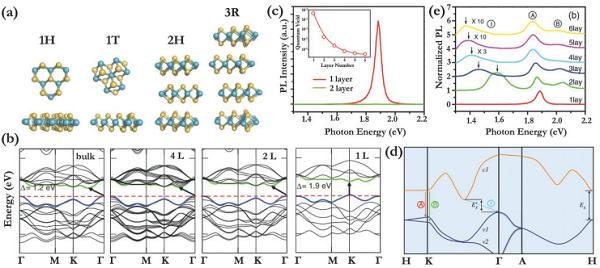
(a) The crystal structure of the MoS2 isomorph; (b) the evolution of the MoS2 band structure of the triangular prism coordinate from a block to a single layer; (c) the photo-emission spectra of single and two-layer MoS2; (d) ) Schematic diagram of splitting MoS2 valence band, direct band gap and indirect band gap transition emission; (e) Normalized photoemission spectrum of MoS2 evolves with layer thickness.
Figure 5. Intrinsic structure and luminescent properties of black phosphorus

(a) the lattice structure of black phosphorus with a single layer thickness of 5.3 Å; (b) the quasiparticle band structure of phosphene calculated by the GW-BSE method; (c) when incident light is irradiated along the x direction, Absorption spectrum of phosphene; (d) Anisotropic reflection spectrum of phosphene under polarized light irradiation in x and y directions; (e) Polarization resolution of phosphene under polarized light irradiation at 532nm in x or y direction (F) When the polarization angle of the incident laser light is 0 °, 45 °, and 90 °, the change in the intensity of the phosphorescent photoemission spectrum in the polarization detection direction of 0 ° to 360 °; (g) Phosphene (H) on the schematic diagram of the relationship between the quasiparticle band gap of phosphene and exciton emission energy; below: consider (exciton absorption) and not consider separately (Quasiparticle Absorption) The theoretically calculated optical absorption spectrum of phosphene when carriers interact.
Figure 6. Electronic structure and emission characteristics of black phosphorus layer thickness

(a) the evolution of the black phosphorus band structure with increasing layer thickness; (b) the normalized photoluminescence emission spectra of black phosphorus from 1 to 5 layers; (c) the peak energy (optical band gap) and The number of layers.
Figure 7. Electronic structure and luminescence characteristics of black phosphorus layer thickness
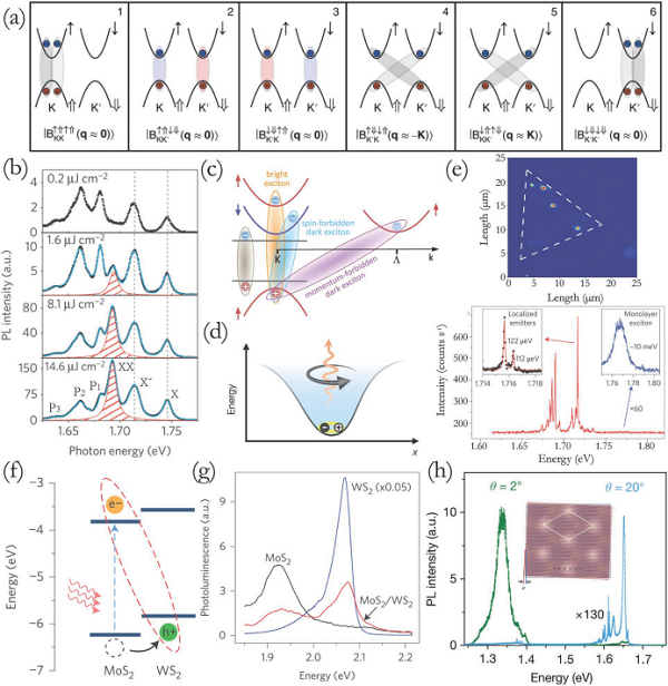
(a) Dual exciton configuration; (b) Variation of light-induced emission spectrum of single-layer WSe2 with light intensity under ultrafast pumping light irradiation; (c) Bright and dark exciton (including spin (Dark excitons forbidden and momentum forbidden) Configuration diagram; (d) Schematic diagram of local exciton captured in space; (e) Single-layer WSe2 local exciton emission; (f) MoS2 / WS2 heterojunction in type II Schematic diagram of interlayer exciton formation; (g) Photoluminescence spectra of single-layer MoS2, single-layer WS2, and MoS2 / WS2 vertical heterojunctions; (h) MoS2 / when the interlayer tilt angle is 2 ° and 20 ° Photoluminescence spectrum of WS2 heterojunction.
Figure 8. Two-dimensional material emission control strategy
Figure 9. Luminance regulation based on size engineering
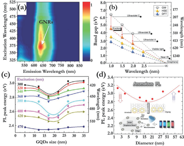
(a) Photoluminescence profile of graphene nanoribbons sealed in single-walled carbon nanotubes; (b) Graphene quantum dot band gap and exciton emission and quantum calculated based on GW, HSE, and traditional DFT calculations Relationship of dot diameter; (c) Size dependence of graphene quantum dot photoluminescence energy under different wavelength excitations; (d) Synergistic effect of quantum confinement effect and edge microstructure on graphene quantum dot photoluminescence.
Figure 10. Lighting control based on defect engineering
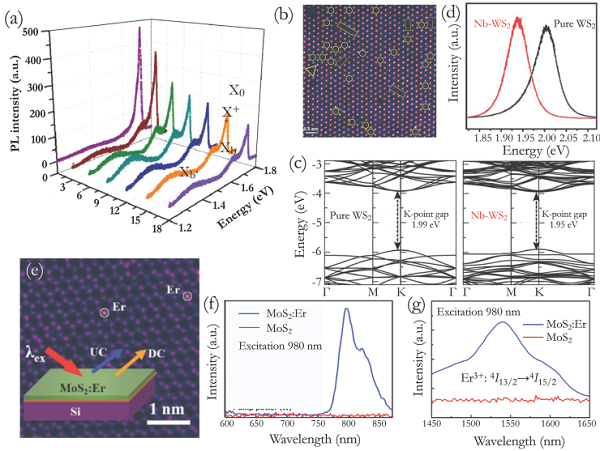
(a) Photoluminescence spectra of single-layer WSe2 treated with Ar + plasma at different times; (b) Spherical aberration-corrected scanning tunnel electron microscope images of Nb-doped single-layer WS2; (c) DFT theoretical calculation of single-layer WS2 and Nb Band structure of doped single-layer WS2; (d) Photoluminescence spectra of single-layer WS2 and Nb-doped single-layer WS2; (e) Spherical aberration correction scanning tunnel electron microscope image of rare earth ion Er3 + doped single-layer MoS2; (F) up-conversion and (g) down-conversion photoluminescence spectra of Er3 + doped single-layer MoS2 excited by 980nm infrared light.
Figure 11. Alloying luminescence regulation of two-dimensional materials
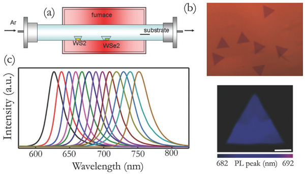
(a) Schematic diagram of WS2xSe2 (1-x) alloy nanosheets prepared by CVD method; (b) Triangular appearance of WS2xSe2 (1-x) alloy nanosheets and photoluminescence diagrams of individual nanosheets observed by an optical microscope; (c) Photo-induced emission spectra of the composition-dependent WS2xSe2 (1-x) alloy nanosheets.
Figure 12. Chemically functionalized luminescence regulation of two-dimensional materials
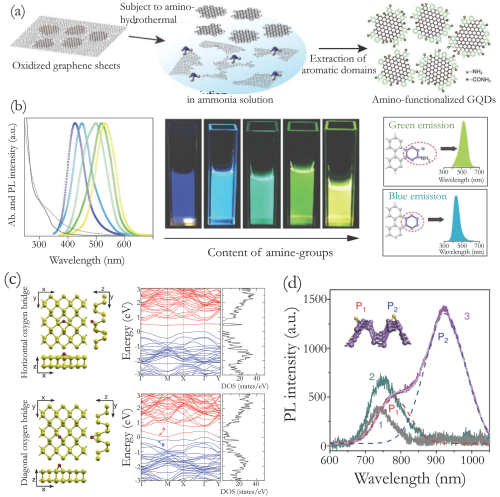
(a) Schematic diagram of the preparation of aminated graphene quantum dots by the ammonia method; (b) The emission spectra (left) and luminescence photos (middle) of graphene quantum dots with different degrees of amination under ultraviolet light excitation at 365 nm, and Possible edge microstructures for blue and green emission; (c) Horizontal bridge oxygen (top) and diagonal bridge oxygen (bottom) configurations and corresponding electronic band structure and density of states in the phosphene lattice; ( d) Photoluminescence spectra of phosphene, phosphene covering the PxOy layer by oxygen plasma etching, and over-etching of phosphorene.
Figure 13. Chemically functionalized luminescence regulation of two-dimensional materials
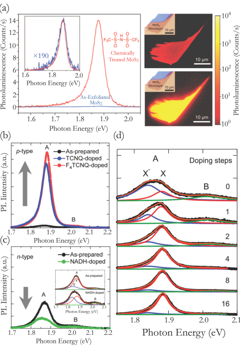
(a) Photoluminescence spectrum (left) and luminescence scan (right) of a single-layer MoS2 nanosheet before and after functionalization with TFSI; (b) Before and after functionalization with p-type dopants (TCNQ and F4TCNQ) Photoluminescence spectrum of single-layer MoS2; (c) Photoluminescence spectrum of single-layer MoS2 before and after functionalized with n-type dopants; (d) Photoluminescence spectrum of F4TCNQ functionalized single-layer MoS2 as a function of dopant concentration Increased evolution.
Figure 14. Electrostatic and carrier injection luminescence regulation of 2D materials
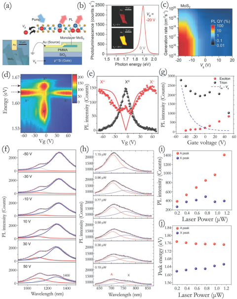
(a) Schematic diagram of single-layer MoS2 supercapacitors regulating the formation and generation rate of different quasi-particles by electrostatic; (b) When the photocarrier rate is G = 1018 cm-2 s-1 and the gate voltage Vg = -20 and 0 V , The photoluminescence spectrum of a single-layer MoS2 supercapacitor; (c) single-layer MoS2 quantum yield distribution function as a function of G and Vg; (d) single-layer MoSe2 under different gate voltages excited by 1.73 eV laser (E) Variation of exciton and tri exciton emission intensity with gate voltage in single-layer MoSe2; (f) Three-layer phosphorene gate voltage-dependent photoemission spectrum; (g) Three-layer Variation of exciton and tri exciton emission intensity in phosphene with gate voltage; (h) Photoluminescence spectrum of phosphorene excited by lasers with different powers; (i) Luminous intensity and (j) Evolution of luminous energy with laser power .
Figure 15. Luminescence regulation of a two-dimensional material with a magnetic field
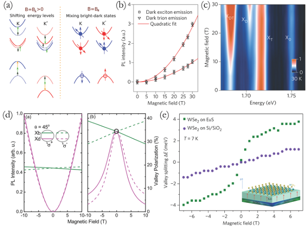
(a) Schematic diagram of the changes in the single-layer WSe2 valley structure and electron spin in the vertical magnetic field (left) and parallel magnetic field (right); (b) the luminous intensity of the dark exciton and dark triple exciton in the single-layer WSe2 and Dependence of parallel magnetic field strength; (c) Scanning of the emission energy of exciton (X0), triple exciton (XT), dark exciton (XD), and dark triple exciton (XDT) in a single layer of WSe2 as a function of parallel magnetic field strength (D) When the magnetic field tilt angle is 45 °, the change law of the emission intensity and valley polarizability of the bright exciton and dark exciton in the single-layer WSe2 with the magnetic field intensity; (e) the pair of SiO2 / Si substrate and EuS substrate Effect of Magnetic Separation in Single Layer WSe2 Valley Splitting.
Figure 16. Two-dimensional material strain emission control
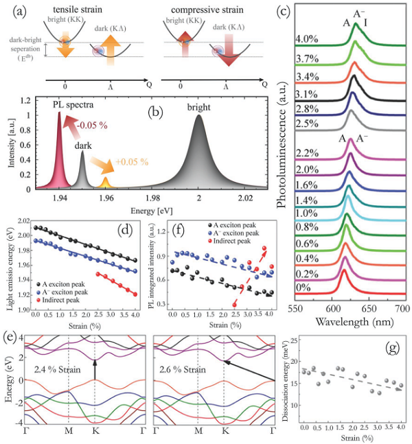
(a) The effects of tensile and compressive strains on the energy interval between bright and dark exciton states in a single layer of WS2; (b) The effects of tensile and compressive strains on the resonance emission spectra of bright and dark excitons; c) Single-layer WS2 photoemission spectrum under uniaxial tensile strain with different intensity under 532nm laser irradiation; (d) Exciton, triple exciton and indirect band gap emission peak energy in single-layer WS2 are pulled along with uniaxial Variation of tensile strain; (e) Band diagram of single-layer WS2 when uniaxial tensile strain is 2.4% and 2.6%; (f) Excitons, triple excitons, and indirect band-gap emission in single-layer WS2 Changes in peak integrated intensity and (g) triple exciton dissociation energy with uniaxial tensile strain.
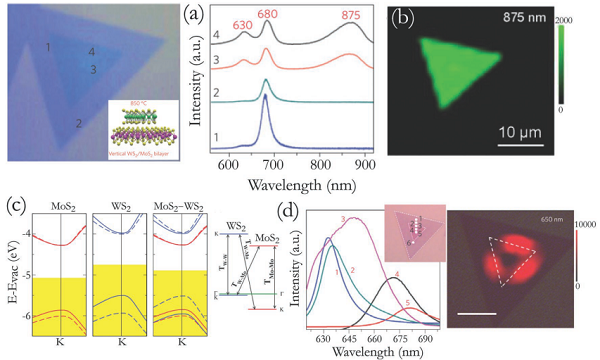
Figure 17. Luminescence regulation of 2D material heterojunction
(a) Optical images of WS2 / MoS2 vertical heterojunction (left), and emission spectra of single-layer MoS2 (points 1 and 2) and double-layer heterojunction regions (points 3 and 4) (right); b) Luminous energy scan of WS2 / MoS2 vertical heterojunction when the emission peak is 875nm; (c) Band structure of single-layer MoS2, single-layer WS2 and double-layer WS2 / MoS2 heterojunction at point K, And the electron transition channels that cause additional emission peaks to appear in the heterojunction; (d) the emission spectrum of the lateral WS2 / MoS2 heterojunction (left), and a scan of the local emission at the interface of the heterojunction.
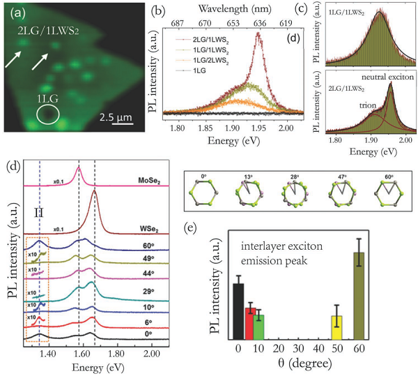
Figure 18. Effect of layer number and tilt angle on the luminescent properties of 2D material heterojunction
(a) Luminescence scan of WS2 / graphene heterojunction with 2LG / 1LWS2 heterojunction at the bright spot; (b) Emission of single-layer graphene, single-layer WS2, 1LG / 1LWS2, 1LG / 2LWS2, and 2LG / 1LWS2 Spectrum; (c) Deconvoluted peak analysis of 1LG / 1LWS2 and 2LG / 1LWS2 emission spectra; (d) MoSe2, WSe2, and MoSe2 / WSe2 with relative twist angles of 0 ° -60 ° under laser excitation at 488 nm Emission spectrum of vertical heterojunction; (e) Variation of MoSe2 / WSe2 vertical heterojunction emission intensity with twist angle.
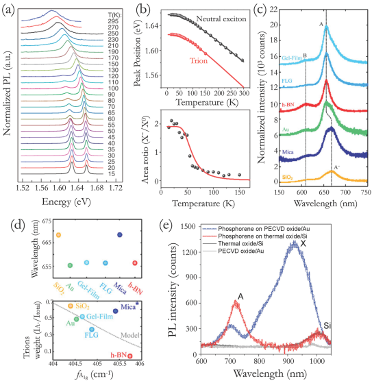
Figure 19. Effect of temperature and matrix on the luminescent properties of 2D materials
(a) Normalized emission spectra of single layer MoSe2 excited by 1.96 eV laser at different temperatures; (b) Exciton and triple exciton emission peaks in single layer MoSe2 (above), and their integrated area ratio with temperature (C) the emission spectrum of a single layer of MoS2 based on a gel film, a few layers of graphene, h-BN, Au, mica, and SiO2; (d) the maximum emission intensity of a single layer of MoS2 from different substrates and The effect of the triplet exciton weight with the change of A1g Raman vibration mode; (e) Photoluminescence spectra of phosphene deposited on PECVD oxidation / Au substrate and thermal oxidation / Si substrate, respectively.
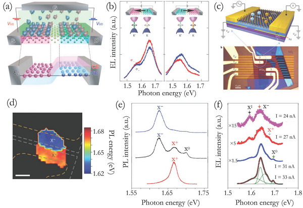
Figure 20. Application of two-dimensional materials in light-emitting diode devices
(a) Schematic diagram of the structure of an electric double layer light-emitting transistor (EDLT) based on WSe2 and the band structure of a pin junction formed in the EDLT; (b) The electroluminescence spectrum of the EDLT device when the current direction is opposite; c) Single-layer WSe2 pn junction light-emitting diode device structure (top) and optical microscopy (bottom); (d) Photoluminescence energy scan of lateral pn junction; (e) p-type doped, n Emission spectrum of the doped and pn junction regions. The p-type region is a negative tripletron emission, the n-type region is a positive tripletron emission, and there are both exciton (X0) and negative triplet exciton (X-) in the pn junction region. And positive triple exciton (X +) emission; (f) the electroluminescence spectrum of the lateral pn junction at different current intensities;
Figure 21. Laser applications of 2D materials
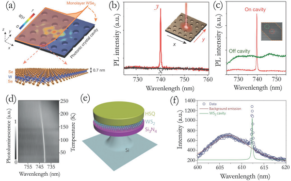
(a) Schematic diagram of the structure of a photonic crystal nanoresonator laser based on a single layer of WSe2; (b) Polarization-resolved photoluminescence spectrum of a nanoresonator laser under 632 nm laser excitation; (c) A nanoresonator laser and off-resonance nanoresonance Comparison of emission spectra in the cavity region; (d) Photoluminescence distribution of nano-cavity lasers as a function of temperature; (e) Schematic diagram of HSQ-WS2-Si3N4 sandwich microdisk lasers; (f) Photoluminescence spectra of WS2 resonators;
Figure 22. Biological imaging and biosensing applications of two-dimensional luminescent materials
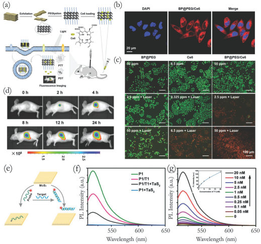
(a) Schematic diagram of the preparation of Ce6 modified BP @ PEG photosensitizer and its cancer diagnosis and treatment mechanism; (b) Fluorescence imaging of HeLa cells after incubation with BP @ PEG nanosheets; (c) When laser radiation is present and without laser radiation, Comparison of fluorescent imaging effects of BP @ PEG nanosheets, Ce6 and Ce6 modified BP @ PEG nanosheets on HeLa cells; (d) Changes in fluorescent biological imaging of Ce6 modified BP @ PEG nanosheets in mice over time; (e ) Schematic diagram of DNA biological detection mechanism; (f) Effects of TaS2 nanosheets on FAM-labeled single-stranded DNA and H1N1 virus-bearing single-stranded DNA photoemission spectra; (g) Sensitivity of TaS2-based biosensor emission spectrum to H1N1 virus concentration Sex
【summary】
New properties triggered by quantum confinement effects, including tunable electronic structures, strong light-matter interactions, high carrier mobility, and a wide range of spectral applications, make 2D materials stand out in the field of light emission and form the basis of light emission physics Research and applications of high-efficiency light-emitting devices provide novel perspectives. In order to better understand the physical basis of luminescence of two-dimensional materials and broaden the application of luminescence of two-dimensional materials, researchers have proposed various theoretical and experimental studies on two-dimensional materials‘ luminescence control strategies. This article not only provides a broad overview of these luminescence regulation strategies, but also provides an overview of the geometry and electronic structure of various leading-edge two-dimensional materials, exciton physics, luminescence applications and challenges.
[Article Information]
Inorganic 2D Luminescent Materials: Structure, Luminescence Modulation, and Applications
Liumei Su, Xing Fan, Teng Yin, Huide Wang, Yu Li, * Fusheng Liu, Junqin Li, Han Zhang, * Heping Xie
(Adv. Opt. Mater., 2019, 1900978. DOI: 10.1002 / adom.201900978)
Source of information: material cattle