

Research Background
Doping of semiconductor TMDs is an effective method to adjust their physical and chemical characteristics, and finally provides more functions for devices based on complex nano-architectures. One of the most effective ways to achieve TMDsdoping is to replace transition metal atoms in the TMDs lattice. Since this doping method involves a chemical bond (usually a covalent bond) between the doped atom and the host lattice, it is more stable and less volatile than the surface charge transfer doping by physical adsorption. By doping, the carrier density and electrical doping type can be changed . Previous reports have shown that the introduction of Nb atoms into the MoS 2 lattice leads to stable p-type transport, while Re and Fe doping leads to n-type behavior. Recent theoretical and experimental studies have also shown that ferromagnetism can be induced by doping transition metal elements (including Mn, Fe, Co, and Zn) in TMDs . In addition, by doping and alloying of two different TMDs , the catalytic performance of semiconductor TMDs is improved. In addition, by constructing heterojunctionsbased on doped -undoped TMDs or two pure phases involving different TMDs, two -dimensional pn junction FETs and photovoltaic devices have been successfully prepared .
Commonly used to dope a three-dimensional ( 3D) semiconductor diffusion and ion implantation method is not suitable for atomic thin the TMD S , because the required high temperature process and / or ion bombardment leads to one orfew layers in the form of the TMD S rapid degradation. In contrast, may TMDs ofgrowth process using in-situ doping of the method , is more suitable for obtaining thin dopant atoms substituted with the TMD S .
Achievements
In view of this, recently, Professor Mauricio Terrones and Ana Laura Elías (co-corresponding author) of Pennsylvania State University , USA , have been inspired by the sol-gel process to jointly report on the use of liquid-phase precursor assisted methods for single-layer TMDs and doping concentrations Adjustable in-situ heterojunction instead of doping . This highly repeatable approach is based on high temperature vulcanization of a spin-on aqueous solution containing a host and a dopant precursor. Before the synthesis process, the precursors are uniformly mixed in the liquid phase, thereby improving the uniformity and controllability of the doping. It is further proved that various transition metal atoms (such as Fe, Re, and V) can be doped into the TMD single-layer lattice to form Fe-doped WS 2 , Re-doped MoS 2 and more complex material systems, such as V-doped In-plane W x Mo 1-x S 2 -Mo x W 1-x S 2 heterojunction.The method developed in this paper is universal and can be extended to doping various other elements into 2D TMDs and constructing in-plane heterogeneous interfaces in one step, making the application of 2D limits (such as electronics and spintronics) possible. . The article was published in the famous journal ACS Nano under the title " Universal In Situ Substitutional Doping of Transition Metal Dichalcogenides by Liquid Phase Precursor-Assisted Synthesis ".on.
Graphic guide

Figure 1. Liquid-phase precursor-based method for doping TMDs. (A) Flow diagram of 2D TMDs and in-plane heterojunction substitution doping. By appropriately selecting and mixing water-soluble compounds as precursors, doped TMDs and in-plane heterojunctions can be synthesized accordingly. (B) A schematic diagram of the selection of doped TMDs system and the principle of dopant selection.
Figure 1a depicts an overall flowchart of a liquid-phase precursor-assisted synthesis method. In short, the method involves spin coating an aqueous solution containing a transition metal precursor and sodium cholate onto a SiO 2 / Si substrate, followed by a high temperature vulcanization process. Sodium cholate is used as a surfactant to help adhere the precursor to the SiO 2 / Si substrate during the spin coating process . Figure 1b shows the researched doped TMDs system, including single-layer Fe-doped WS 2 , Re-doped MoS 2 , V-doped WS 2 and V-doped Mo x W 1-x S 2 -W x Mo 1- x S 2 In- plane heterojunction. It is worth mentioning that the basic principles of selecting these doped TMD systems include three aspects: (1) Since precursors need to be mixed in the liquid phase, there should be readily available water-soluble compounds as dopant precursors. (2) Compared with Mo and W, doped atoms should have a larger difference in atomic Z number. (3) Compared with the transition metal atoms in the host lattice, the dopants should have similar or slightly smaller atomic radii, so as to ensure minimal lattice strain when introducing doped atoms into TMDs.

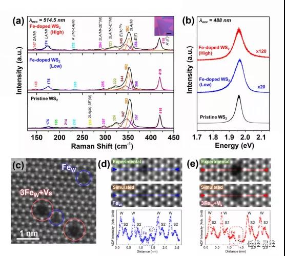
Figure 2. Single-layer Fe-doped WS 2 . ( A ) The Raman spectra of Fe doped WS 2 and original W S 2 (normalized to A ‘ 1 ( Γ) mode) with two different doping concentrations were compared using a 514.5 nm laser . (B) PL spectra of Fe-doped W S 2 and original W S 2 monolayers . (C) Atomic-resolved STEM-ADF image of a single-layer Fe-doped W S 2 (high doping level) . (D & e))Experimental and simulated STEM images and line scans of Fe W and 3Fe W + V S dopant configurations .
First, Fe doped W S 2 was synthesized using ammonium metatungstate ( AMT) and FeCl 3 as precursors of W and Fe . In order to study the tunability of the doping concentration, two different concentrations of FeCl 3 precursor solutions(ie, "low-doped" and "highly-doped") were used. Figure 2a shows the optical image of the synthesized single-layer Fe-doped W S 2 with a triangular morphology and a lateral dimension of about 100 μm. Under resonance conditions (excitation with a 514.5 nm laser) , Raman spectra of a single-layer original W S 2and two Fe-doped W S 2 with different doping concentrations were obtained , asshown in Figure 2a. The Raman spectrum is normalized to the intensity of the A ‘ 1( Γ) mode. The original W S 2 exhibited obvious first-order vibration modes ( E ‘ ( Γ) and A ‘ 1 at 357 cm -1 and 419 cm -1 , respectively ).( Γ) ). In contrast, with the Fe-doped increases, E ‘ ( Gamma]) and A ‘ . 1 ( Gamma]) mode, red-shifted, and the high Fe-doped W is S 2 of the two modes are appeared . 1 cm & lt -1 of Redshift.The observed Raman frequency shift comes from both the lattice strain andthe charge doping effect caused by Fe doping. Except for the first-order mode, all spectra obtained under resonance conditions contain several higher-order Raman modes and combined modes, which are identified in Figure 2a. In order to study the optical properties of WS 2 monolayer after Fe doping, room-temperature photoluminescence ( PL) characterization was also performed (Figure 2b). The results show that light and high Fe doped W S 2The PL spectra were significantly broadened. In addition, their intensity gradually decreases with the increase of the doping concentration, where the lightly and heavily doped PL strengths are respectively higher than the original W S 2Reduced by about 20 times and 120 times. Fe doping may introduce deep-level defect states, resulting in non-radiative recombination of photo-excited carriers, and thus PL quenching.
A representative HAADF-STEM image of Fe-doped W S 2 (highly doped) isshown in Figure 2c, where Fe atoms have a relatively low atomic Z number and appear as darker atoms occupying the W position. Two main types of dopant configurations can be found in the STEM-ADF image, one is a single Fe substitution (Fe W ) in the W position, and the other is a three Fe substitution (3FeW + V with sulfur vacancies in the middle) S ). FIGS. 2d and e are given of Fe W isand 3Fe W is + V S experimental and simulated STEM image and line scan results show a good match of the two types of dopants configuration. It is worth noting that for 3Fe W + V S , it is observed that the position of the Fe-doped atom is different from the position of the W atom in the original WS 2 lattice , and sulfur atoms opposite to the vacancies move into the transition metal plane, resulting in 3 Fe atoms from The center of the vacancy moves to the other sulfur pair to which it is bonded.

Figure 3. Single-layer Re-doped Mo S 2 . ( A) Optical image of a single-layer Re-doped Mo S 2 sheet. ( B) using the 488 nm original laser beam and Re obtained by doping of Mo S 2 Raman spectrum (normalized to A ‘ . 1 mode). (C) PL spectra of Re-doped Mo S 2 and original Mo S 2 monolayers . (D) Atom-resolved STEM-HAADF image of a single layer of Re-doped Mo S 2synthesized with AHM: APR 1: 1 (low doping) . (E) Experimental and simulated STEM images and line scans of Re Mo dopants . (F) Single-layer Re-doped Mo S 2 synthesized with AHM: APR 1:10 wt (highly doped)Atomic-resolved STEM-HAADF images. Interestingly, the increase in the number of Re-doped precursors leads to 1T‘-Re S 2 in the local areaAnd 1H-Mo S 2A heterogeneous interface is formed.
Re-doped Mo S 2 was synthesized using ammonium paramolybdate ( AHM) and ammonium perrhenate (APR) as the precursors of Mo and Re, respectively .Samples synthesized with two different metal concentration ratios were studied, namely AHM: APR 1: 1 wt (low doping) and 1:10 wt (high doping). Figure 3a shows an optical image of a single layer of Re-doped Mo S 2 , showing a triangular shapewith a lateral dimension of about 20 μm. Figure 3b shows the Ra-doped spectra ofthe Re-doped and original Mo S 2 , both showing two distinct first-order vibration modes ( E ‘ and A ‘ 1 ). Compared with the original Mo S 2 , the frequency of the E‘ mode in the Re-doped MoS 2 does not change significantly, but the A ‘ 1 mode is red shifted by 1 cm -1 . It has been found previously that the frequency of the E‘ mode in MoS 2 is relatively insensitive to doping, but due to MoS2 strong electron - phonon coupling, A ‘ . 1 mode tends to soften at high electron doping concentration, therefore, A ‘ . 1 pattern offset may be due to electron-induced dopant doping Re. The room temperaturePL study showed that the PL of the single-layer Re-doped MoS 2 wasredshifted by 20 meV and quenched by more than 5 times (Figure 3c). The n-type doping can effectively reduce the spectral weight of excitons, resulting in PL emission dominated by negative triplets.
Atomic-resolved STEM-HAADF imaging was performed to confirm that the Re substitution was doped into Mo S 2 (Fig. 3d). Relying on the Z contrast, the Re atom was prominently displayed as a bright atom at


