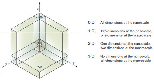
One classification of nanomaterials is based on the size of the material, which is outside the nanoscale (<100 nm) range.
Therefore, in zero-dimensional (OD) nanomaterials, all dimensions are measured in the nanometer range (no dimensions greater than 100 nm). Most commonly, OD nanomaterials are nanoparticles.
In one- dimensional nanomaterials (1D), one dimension is outside the nanoscale. This category includes nanotubes, nanorods and nanowires.
In two-dimensional nanomaterials (2D), two dimensions are not in the nanometer range, while one dimension is only one or a few atomic layers thick. This class exhibits a plate-like shape, including graphene and other single-layer materials, such as MXenes , black phosphorophosphene , and diatomic hexagonal boron nitride.
Three-dimensional nanomaterials (3D) are nanoscale materials that are not limited to any size. This class can include bulk powders, dispersions of nanoparticles, nanowire bundles, nanotubes, and multilayer nanolayers.
Classification of nanometer sizes. (Source: Tallinn University of Technology)
What makes 2D materials so interesting to researchers is their excellent physical and chemical properties compared to a large number of similar materials.
Inspired by the unique optical and electronic properties of graphene, in recent years, two-dimensional layered materials and their hybrid materials have been extensively studied, mainly due to their potential applications in the field of nanoelectronics.
Atomic layered crystals have a wide spectral range, including transition metal carbon disulfide (TMD), semiconductor carbon disulfide, monoatomic buckling crystals such as black phosphorus (BP or phosphorus) and diatomic hexagonal boron nitride (h-BN).
Such materials can be obtained by exfoliating bulk materials into small scales, or by large-area epitaxial growth and chemical vapor deposition (CVD).
This atomically thin monolayer or monolayer crystal has strong intralayer covalent bonds and weak interlayer van der Waals bonds, thus having excellent electrical, optical and mechanical properties.
Source of information: Nanowerk