[Special] surface energy assisted method transferring two-dimensional material
The surface energy assisted transfer method [or liquid wedge method] was first reported by Professor Cees Dekker‘s group in the 2010 document "Wedging Transfer of Nanostructures" [1] . The different surface energies of the substrate and the two-dimensional material can drive water molecules to penetrate into the interface between the substrate and the material , thereby separating the two-dimensional material from the substrate, and the solid surface is called surface energy assisted transfer. The surface energy assisted transfer method is especially useful for separating and transferring two-dimensional materials from difficult-to-corrode substrates, or reducing the contamination of impurities during the material transfer process, and has the effect of turning decay into a magic. As shown in Figure 1, the earliest reported method of surface energy assisted transfer. This article reports that the glass sheet spin-coated with hydrophobic polymer inserted into water at a certain angle will cause the polymer to detach from the substrate under the action of water and float in the water. On the surface. The article further applies this method to the exfoliation of two-dimensional materials, and transfers the exfoliated two-dimensional materials to a specific position above the target sink bottom to achieve the fixed-point transfer of graphene and other nanomaterials.

Figure 1 The hydrophobic polymer layers on both sides of the glass slide are separated from the substrate and float on the water
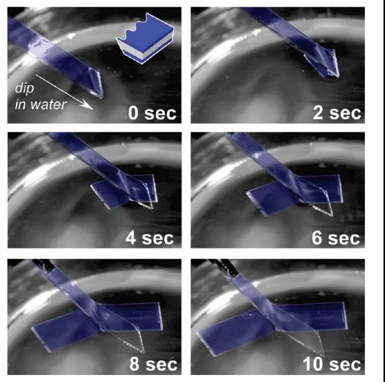
The mechanism of separating the two-dimensional material from the substrate is as follows: Because the substrate (glass, quartz, SiO2, etc.) is hydrophilic, water will quickly infiltrate the substrate surface, but the polymer is hydrophobic and will repel water. Water is inserted between the hydrophilic substrate and the hydrophobic polymer between the interface and separates the polymer and the substrate. At the same time, the hydrophobic two-dimensional material also falls off the substrate together with the polymer. The method shown in Figure 2 can realize the fixed-point transfer of two-dimensional materials. Figure 2A shows the transfer device used in the article [1]. Put the target substrate in a Petri dish containing water, and then float the polymer with the two-dimensional material on the substrate through the surface energy assisted method, and transfer it to the optical microscope to observe the position of the two-dimensional material in real time. Use a pipette to slowly absorb the water in the petri dish, so that the polymer slowly approaches the target sink. When the polymer is close enough to the substrate, the position of the polymer can be manipulated by a probe fixed on the three-axis stage to move The two-dimensional material moves above the target position of the substrate and slowly adheres to complete the transfer.

Figure 2B-E shows the process of two-dimensional material detached from the substrate, transferred, and approached, and the final target position is fitted
As shown in FIG. 2F, a conceptual diagram of the transfer process, the surface energy assisted method can penetrate water molecules to the interface between the polymer and the substrate, and realize the separation and floating of the two-dimensional material and the substrate on the water surface. The probe fixed by the three-axis stage can finely adjust the horizontal position of the two-dimensional material by external force, and can also realize the bonding of the two-dimensional material and the substrate by regulating the movement in the vertical direction, and realize the fixed-point transfer of the two-dimensional material. This method can realize the transfer of a series of nanostructures, such as the transfer of metal electrodes and the transfer of nanostructure patterns, and it can also realize the transfer on uneven surfaces such as spherical substrates.
As shown in FIG. 2F, first, the surface energy assist method is used to detach the two-dimensional material from the substrate and float on the surface of the water together with the polymer. After removing a certain amount of water with a pipette, when the vertical distance between the polymer and the substrate is close enough, the position of the polymer and the two-dimensional material can be controlled by the probe mounted on the stage, and the target material can be transferred to a specific position above . This method can realize the transfer of a series of nanostructures, such as the transfer of metal electrodes and the transfer of nanostructure patterns.

Figure 2F Using wedging transfer to implement a fixed-point transfer method for multilayer graphene
In 2014, Professor Zhang Hua‘s research group further improved the wedging transfer technology to realize the transfer of different nano-structured materials such as 0D, 1D and 2D. As shown in Figure 3, the specific steps for the transfer of MoS2 reported in the article: ① spin-coated polymer support layer on the MoS2/SiO2/Si L-polylactic acid (poly-l-lactic acid, PLLA), cutting the edge of the support layer to expose the substrate; ② After putting PDMS on top of PLLA, drop a drop of water at the edge. The water drop immerses into the interface between PLLA and SiO2 and peels off PDMS/PLLA/MoS2 from SiO2/Si, and then transfers to the target substrate; ③ Heat to peel off PDMS, 50℃ methylene chloride Dissolve PLLA, wash and dry to complete the transfer. Compared with the transfer method of wet dissolving the substrate, this method reduces the bubbles generated during the transfer process and the stress generated when the film is taken out, and can achieve rapid transfer.

Figure 3 Schematic diagram of Wedging transfer nanostructure.
In the same year, Prof. Linyou Cao‘s research group developed a simpler method of assisting transfer of surface energy. Using the support layer polystyrene (PS), the transfer of large-area MoS2 thin films synthesized on sapphire substrates was successfully achieved. The process is shown in Figure 4.
The steps are:
① After spin coating PS on MoS2/sapphire, drop a layer of water droplets, and cut the edges of the sample to leave gaps on the side of MoS2/SiO2. Because MoS2 is hydrophobic and sapphire is hydrophilic, the water droplets automatically penetrate into the interface between MoS2 and the substrate. Make MoS2 slowly detach from the growth substrate; ② Transfer the PS layer with MoS2 directly to the target substrate; ③ Dissolve PS with toluene to complete the transfer.
As shown in Figure 5, this method can transfer two-dimensional materials over a variety of substrates. Figure 5a shows a photograph of a MoS2 film grown on a sapphire substrate transferred to a silicon wafer. Figures 5d, e, f, and g are photos transferred to the gold film, polyimide film, glassy carbon, and quartz, respectively. And compared with the effect of the substrate etching method (Figure 5h, i), it can be seen that the MoS2 film transferred by the surface energy assisted method has better crystal quality (Figure 5a, b), and the transferred MoS2 film It is continuous and complete.
[Large area transfer] The surface energy assisted 2D transfer method can achieve high crystal transfer quality and has the advantages of simple operation, short transfer time, and no introduction of etching liquid. The preparation of large area 2D device arrays shows great Application potential . Figure 6 shows a schematic diagram of wafer-level two-dimensional material film transfer [5]. The article further improves the use of PDMS instead of PS to eliminate the step of dissolving the polymer in organic solvents and achieve a complete and clean transfer of high-quality films. The specific transfer steps are: ① stick PDMS on the surface of the grown MoS2 film; ② immerse PDMS/MoS2/sapphire together in deionized water. At this time, the water will be immersed in the interface between the substrate and the material, so that PDMS/MoS2 is slowly detached from the sapphire substrate; ③ Remove the PDMS from the water and transfer it to the target substrate to release the MoS2 film. The two-dimensional material pattern can be carved by means of photolithography RIE and other techniques, and the complex stacked structure shown in FIG. 6d can be transferred to prepare a large-area two-dimensional device array.

Figure 6 Transfer of single-layer wafer-level MoS2 film.
Surface energy-assisted transfer utilizes the difference between the surface energy of the two-dimensional material and the substrate, and realizes the separation of the material from the substrate through liquid intercalation, which can facilitate the transfer of high-performance two-dimensional materials, which brings further research and application of two-dimensional materials. great help. This transfer method is suitable for the transfer of a variety of two-dimensional materials obtained by mechanical peeling and CVD synthesis. Especially for the transfer of two-dimensional materials synthesized on substrates that are difficult to dissolve, such as sapphire and mica, it brings great convenience. In short, the surface energy-assisted 2D material transfer method has many advantages, such as simple operation, short consumption time, high quality of transferred crystals, suitable for a variety of 2D materials, and can be prepared in a large area, which brings opportunities for further research and application of 2D materials .
references:
[1] Schneider, Grégory F., et al. "Wedging transfer of nanostructures." Nano letters 10.5 (2010): 1912-1916.
[2] Li, Hai, et al. "A universal, rapid method for clean transfer of nanostructures onto various substrates." ACS nano 8.7 (2014): 6563-6570.
[3] Gurarslan, Alper, et al. "Surface-energy-assisted perfect transfer of centimeter-scale monolayer and few-layer MoS2 films onto arbitrary substrates." ACS nano 8.11 (2014): 11522-11528.
[4] Yu, Hua, et al. "Wafer-scale growth and transfer of highly-oriented monolayer MoS2 continuous films." ACS nano 11.12 (2017): 12001-12007.
This information originates from the Internet for academic exchange only. If infringement please contact us to delete immediately


