
hotline��
17715390137
Tel/Wechat��
18101240246 (Technology)
0512-68565571
Email��mxenes@163.com ��Sales Engineer��bkxc.bonnie@gmail.com
Scan the code to follow or search the official account on WeChat:
2D Materials Fronrier After paying attention,
click on the lower right corner to contact us,
Enter enterprise WeChat.
Professional Services Online

�Ѵ��ļ���photo/1690348366.png
 16903483662.png
Abstract
16903483662.png
Abstract
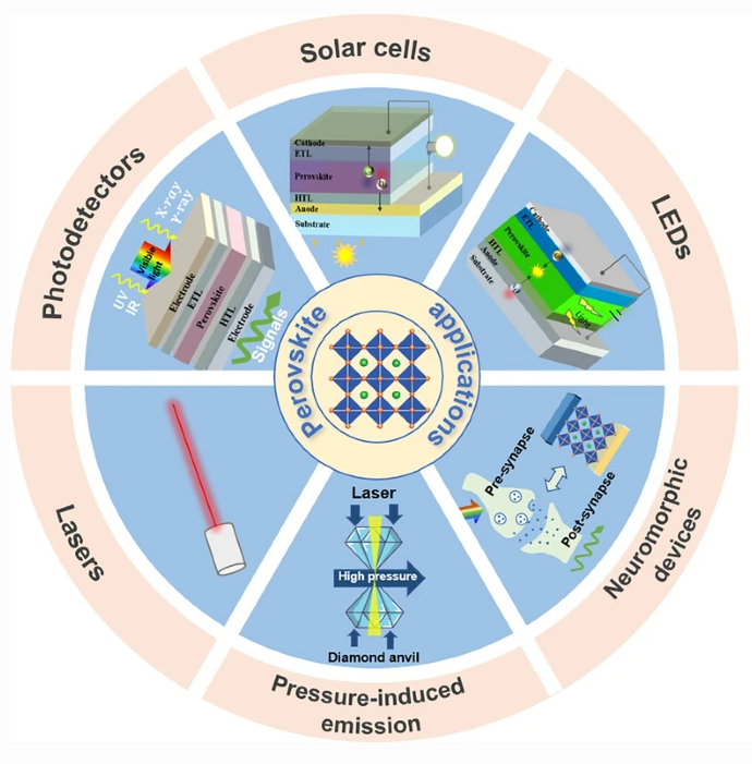
Nowadays, the soar of photovoltaic performance of perovskite solar cells has set off a fever in the study of metal halide perovskite materials. The excellent optoelectronic properties and defect tolerance feature allow metal halide perovskite to be employed in a wide variety of applications. This article provides a holistic review over the current progress and future prospects of metal halide perovskite materials in representative promising applications, including traditional optoelectronic devices (solar cells, light-emitting diodes, photodetectors, lasers), and cutting-edge technologies in terms of neuromorphic devices (artificial synapses and memristors) and pressure-induced emission. This review highlights the fundamentals, the current progress and the remaining challenges for each application, aiming to provide a comprehensive overview of the development status and a navigation of future research for metal halide perovskite materials and devices.
Highlights
A comprehensive summary of the representative promising applications of metal halide perovskite materials, including traditional optoelectronic devices (solar cells, light-emitting diodes, photodetectors, lasers), and cutting-edge technologies in terms of neuromorphic devices (artificial synapses and memristors) and pressure-induced emission.
For each application, the fundamentals of the field, the current progress and the remaining challenges are provided, based on the up-to-date works.
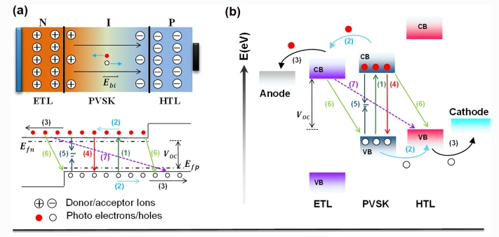
1. Schematic working principle in a P�CI�CN heterojunction and b perovskite solar cells
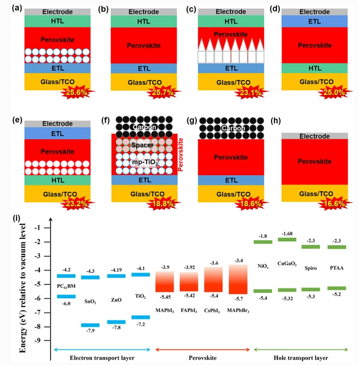
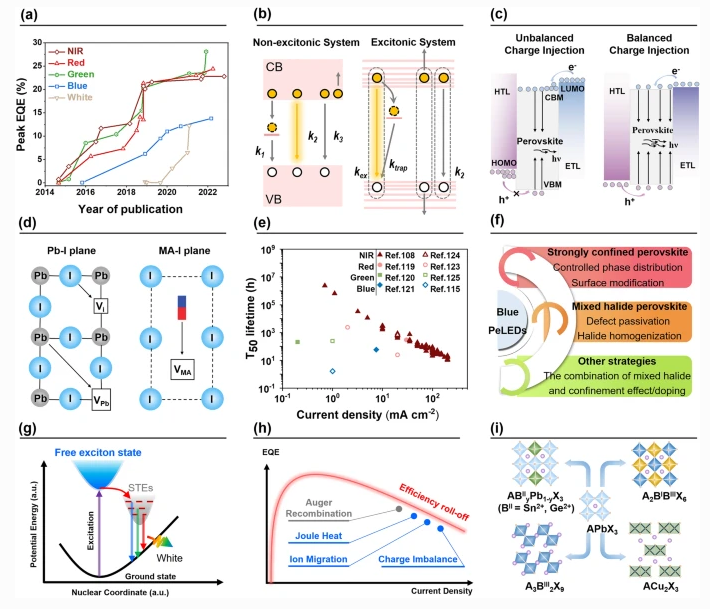
2. Schematic diagram of device architectures and energy level alignment.
3. An Overview of the Field
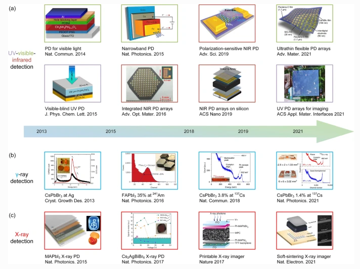
4. Gamma-ray Detectors
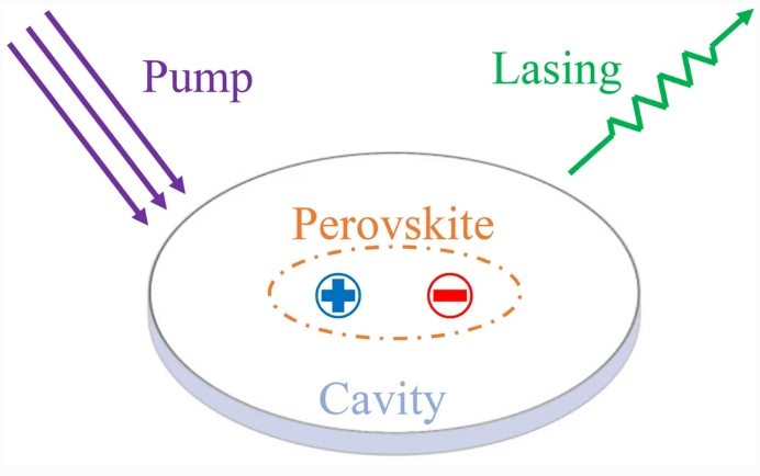
5. Schematic diagram of perovskite laser
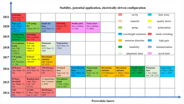
6. Progress timeline of perovskite lasers
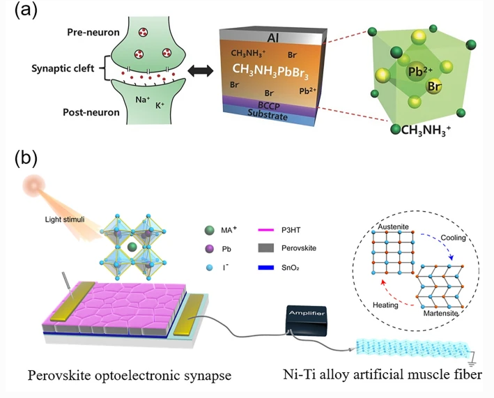
7. a Schematic demonstrations of CH3NH3PbBr3-based perovskite artificial synapse device. b Schematics of an artificial visual nerve mimicking pupil reflex.
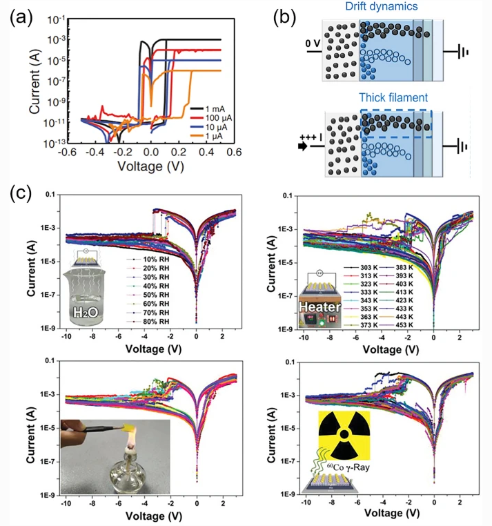
8. Perovskite-based Memristors
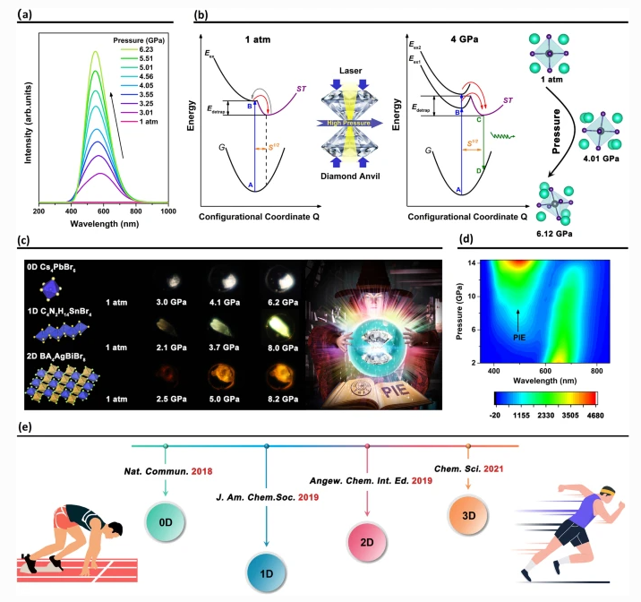
9. Advances of PIE from concept to applications a PL spectra of Cs4PbBr6 NCs under high pressure. b Illustration of PIE mechanism associated with exciton self-trapping in Cs4PbBr6 NCs.
Conclusion
To sum up, we systematically summarized the recent advances and outlined the future challenges for perovskite materials in applications of solar cells, LEDs, photodetectors, lasers, artificial synapses, memristors and pressure-induced emission. Up to now, significant progress has been made in perovskite-based materials and devices. However, there is still plenty of room for further improvement of performance for each application and it is still far away from commercialization. Challenges and opportunities coexist. As a result, a comprehensive knowledge of the current progress, research hot spots and future directions is of vital importance.

| Reminder: Beijing Beike New Material Technology Co., Ltd. supplies products only for scientific research, not for humans |
| All rights reserved © 2019 beijing beike new material Technology Co., Ltd ��ICP��16054715-2�� |
