registered   |   log in
  中文

About us

 
contact us

hotline:

17715390137

Tel/Wechat:

  18101240246 (Technology)
  17319402180 (sales)

0512-68565571

Emailmxenes@163.com (Sales Engineer)bkxc.bonnie@gmail.com

Scan the code to follow or search the official account on WeChat: 

2D Materials Fronrier After paying attention, 

click on the lower right corner to contact us, 

Enter enterprise WeChat.

Professional Services Online

About us
position: home > About us > Industry Information

Materials Today: Large-area fabrication of two-dimensional amorphous alloys and two-dimensional high-entropy alloys

source:beike new material Views:6037time:2020-08-10 QQ Academic Group: 1092348845

【introduction】
In the past ten years, two-dimensional materials such as graphene and molybdenum disulfide have attracted wide attention in the field of materials due to their unique nanostructures and low-dimensional characteristics. Scholars continue to explore the unique physical and chemical properties of two-dimensional materials, and have explored their application potential in high-sensitivity sensors, flexible electronics, and chemical catalysis. In addition to these intrinsic two-dimensional materials with a layered structure, how to reduce the dimensions of metal materials and prepare ultra-thin baseless metal thin films, that is, two-dimensional metals, has also become a hot spot for scientific researchers. The inherent structure of metal materials determines that their existence forms tend to be three-dimensional rather than two-dimensional. Therefore, the preparation process of two-dimensional metal is also relatively tedious and difficult. The existing two-dimensional metal preparation method is mainly based on chemical synthesis in a solution environment. The preparation method is usually directed to a specific single metal element, and the metal growth process is usually slow. Therefore, the chemical composition of the two-dimensional metal that can be prepared is relatively single and the area is small. For multicomponent alloy materials with more complex compositions and structures, such as the widely known metallic glass and the high-entropy alloys that have developed rapidly in recent years, the existing synthesis methods are helpless. As a breakthrough to open the research on the properties of multi-component alloys in low dimensions, the exploration and improvement of two-dimensional complex metal preparation methods have become an urgent need.
[Achievement Profile]
Recently, the team of Professor Yang Yong (corresponding author) of the City University of Hong Kong has made a new breakthrough in the exploration of complex two-dimensional metal preparation methods. Using the newly developed method, a variety of substrate-free two-dimensional metal and ceramic films have been successfully prepared, including Ti. , ZrCuAlNi amorphous alloy, FeCoNiCrNb high entropy alloy, and amorphous silicon, SiC ceramics, Ag-C composite materials, etc. The new preparation method shows wide applicability to a variety of materials. The prepared two-dimensional metals and ceramics also achieved breakthroughs in area scale: Taking two-dimensional Ti as an example, with a thickness maintained at 20 nm, its lateral dimensions can be extended to the macro scale of cm. The aspect ratio is on the order of 106; the thickness of two-dimensional TiO2 can even be as low as 5 nm, and the lateral dimension is also on the centimeter scale. The preparation method is based on a hot-pressed modified polyvinyl alcohol (PVA) polymer, and conventional physical vapor deposition, such as magnetron sputtering, is used as a thin film formation method. The surface instability of the metal-polymer interface under stress is used as the driving force. Force (polymer surface buckling enabled exfoliation, PSBEE), successfully achieved the peeling of metal and ceramic films. In further research, the team found that the preparation method also has good controllability. The peeling behavior of metal films on PVA substrates with different water contents and elastic modulus showed a transition from micro-rolls to large-area films. The experimental results also show that the introduction of coated masks can effectively control the shape and size of two-dimensional metals. Related research results were published in Materials Today under the title "The Controlled Large-Area Synthesis of Two Dimensioanl Metals".

[Picture and text guide]

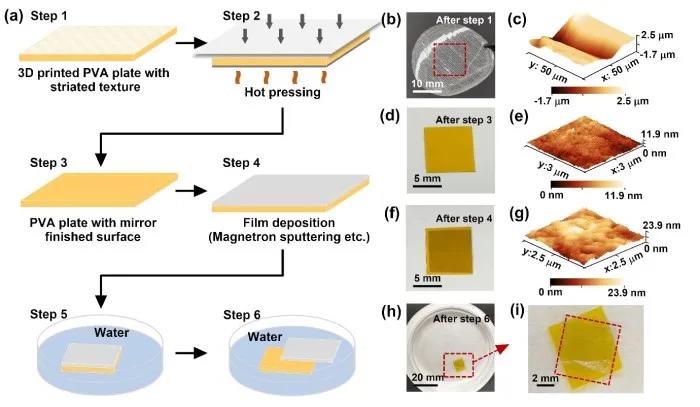
Figure 1. Schematic of a two-dimensional metal preparation method based on PSBEE


a) PSBEE-based two-dimensional metal preparation flow chart based on PVA;
b) 3D printed photos of PVA boards;
c) 3D printed surface morphology of PVA;
d) a real photo of the PVA substrate after hot pressing;
e) Surface morphology of PVA after hot pressing;
f) a real photo of the PVA substrate after the Ti film is deposited on the surface;
g) PVA surface morphology after Ti film deposition;

h) – i) Substrate-free Ti film suspended in water after being peeled from the PVA substrate.

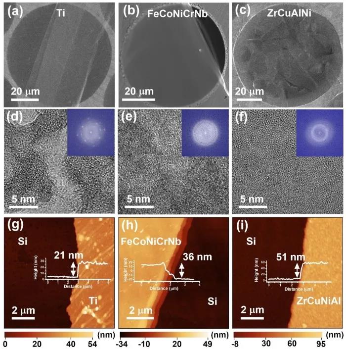
Figure 2. Structural and geometrical characterization of a two-dimensional metal prepared based on this method

a) – c) Scanning electron microscope images of two-dimensional Ti, two-dimensional FeCoNiCrNb, two-dimensional ZrCuAlNi transferred to the copper network;
e) – f) Two-dimensional Ti, two-dimensional FeCoNiCrNb, two-dimensional ZrCuAlNi high-resolution transmission electron microscope pictures, where the built-in pictures are corresponding fast Fourier transform maps;
g) – i) 2D Ti, 2D FeCoNiCrNb, 2D ZrCuAlNi surface morphology at the boundary of the silicon wafer. The built-in curve is a height map sweeping across the 2D metal boundary.

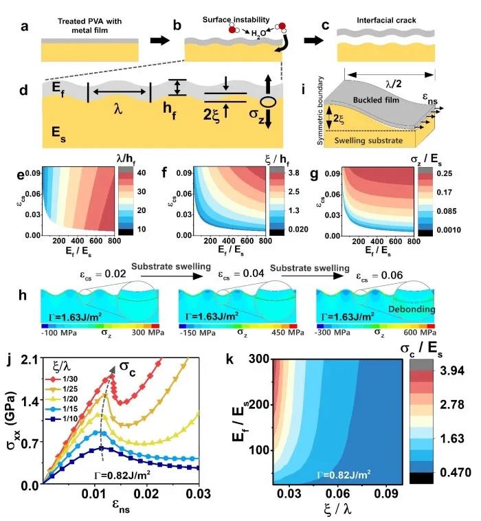
Figure 3. Theoretical description and finite element simulation of the peeling phenomenon caused by surface wrinkles

a) – c) Schematic diagram of the process of diffusion of water molecules into the metal-PVA substrate system to cause surface instability and promote film peeling;
d) a geometric description of the surface of the folds, including the wavelength l of the folds, the amplitude x and the stress sz perpendicular to the plane at the film-substrate interface;
e) – g) contour maps of l / hf, x / hf and sz / Es with ecs and Ef / Es as independent variables
h) Finite element simulation of crack generation at the warped interface of a constrained film-substrate system during expansion;
i) Schematic diagram of interfacial crack growth and expansion during continuous film pulling;
j) the effect of the surface fold geometry on the critical stress in the membrane during crack propagation;
k) Contour map of sc / Es with Ef / Es and x / l as independent variables.

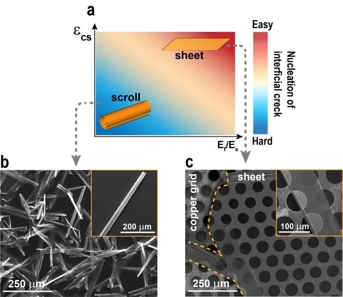
Figure 4. Morphological transition of 2D FeCoNiCrNb from nano-film to micro-roll

a). Schematic diagram of the final morphology change from nano-film to micro-volume under the control of ecs and Ef / Es during the film peeling process. Note that the colors in the figure represent the difficulty of the interface cracks;
b). Image of FeCoNiCrNb microvolume transferred to Si observed under scanning electron microscope;
c). The image of FeCoNiCrNb baseless nano-films transferred to the copper net under a scanning electron microscope.

Figure 5. Regulation of output 2D metal geometry

a) a schematic view of a thin film deposition process with a mask plate involved;
b) – e) actual photo of the mask, the built-in picture is a higher magnification optical microscope image;
f)-h) Scanning electron microscopy images of circular, square and hexagonal 2D FeCoNiCrNb prepared by mask film deposition.

Graphic link:

https://www.sciencedirect.com/science/article/abs/pii/S1369702120300390?via%3Dihub

Website of the research group:
http://www.cityu.edu.hk/stfprofile/yonyang.htm


Reminder: Beijing Beike New Material Technology Co., Ltd. supplies products only for scientific research, not for humans
All rights reserved © 2019 beijing beike new material Technology Co., Ltd 京ICP备16054715-2号
advisory
phone
Email:mxenes@163.com
Tel:+86-17715390137
scan

scan
WeChat