
hotline:
17715390137
Tel/Wechat:
18101240246 (Technology)
0512-68565571
Email:mxenes@163.com (Sales Engineer)bkxc.bonnie@gmail.com
Scan the code to follow or search the official account on WeChat:
2D Materials Fronrier After paying attention,
click on the lower right corner to contact us,
Enter enterprise WeChat.
Professional Services Online

| (Nanowerk Spotlight) Ever since the first demonstration of graphene in 2004, the scientific community has pursued the possibility of building man-made materials by artificial stacking of different ultrathin materials one on top of the other. These materials are called van der Waals heterostructures. | |
| Due to their unique interlayer coupling and optoelectronic properties, these materials are of considerable interest for the next generation of nanoelectronics. | |
| Conventional 2D heterostructures usually are composed of two layers of opposite charge carrier type using inorganic materials. One of the challenges when creating 2D heterostructures is the painstaking stacking of the individual components on top of each other. | |
| Researchers have now found, for the first time, that there can also be charge transfer (CT) induced interfacial coupling between two different pairs of organic CT layers. | |
| Moreover, external stimuli can be harnessed to tune the interfacial coupling to control the physical properties of organic van der Waals heterostructures (vdWHs). | |
| "The interface of heterostructures can provide many possibilities to generate new phenomena," Shenqiang Ren, an Associate Professor in the Mechanical Engineering Department at Temple University, tells Nanowerk. "Our group has years of experience investigating organic CT complexes. As the interface between two layers of organic CT complex is different from the single phase, such as intra-layer and inter-layer CT interactions, it is exciting to investigate the interfacial coupling within organic van der Waals heterostructures." | |
| The most significant finding in this work, just published in Nature Communications ("Tunable two-dimensional interfacial coupling in molecular heterostructures"), is that the researchers found strong and anisotropic interfacial charge transfer coupling in two-dimensional organic van der Waals heterostructures. | |

|
|
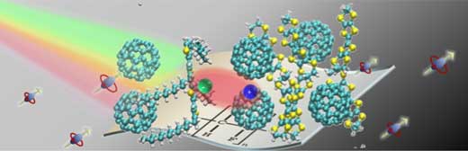
| Organic van der Waals heterostructures exhibit multi-stimuli controlled physical properties. (Image: Dr. B Xu) | |
| As the team (a collaboration between Ren’s group and Prof. Michael L Klein’s High-Performance Computing group at Temple University) points out, such interfacial CT coupling enables external stimuli controlled physical properties in organic vdWHs. | |
| To prepare 2D vdWH, researchers widely use a conventional chemical vapor deposition approach. However, the weak interlayer interaction between the monolayer 2D film and the substrate leads to island growth rather than continuous monolayers. | |
| The approach demonstrated by the Temple University team allows for large-scale (mm2 range) assembly of free-standing 2D CT heterostructures with controlled orientation and unique physicochemical properties. As they note, the interfacial coupling can be tuned over a large range by external fields (ferroelectric and magnetic) with strong enhancement of current and capacitance, due to the coupling across two CT pairs along the vertical and horizontal orientations. | |
| "As our vdWHs show multifunctional external stimuli dependent response (such as piezoresistance, electroresistive and magnetoconductance), they can be applied for multifunctional sensors," says Ren. "For example, the vdWHs exhibit excellent pressure dependent sensitivity with a high piezoresistance coefficient of -4.4×10⁻⁶ Pa-1." | |
| "The organic vdW heterostructures formed by the combination of two pairs of organic CT complex with tunable interfacial coupling show overwhelming advantages over single components," he adds. "They exhibit unique physicochemical properties covering a vast majority of opto-electrical-magnetic-mechanical topics." | |
| The researchers‘ next steps will be focused on the synthesis of wafer-scale two-dimensional vdWHs towards artificial intelligence applications. | |
| Since the organic vdWHs demonstrate a fast response to external stimuli with the change of conductivity, this opens up the practical applications for multi-stimuli sensors. |

| Reminder: Beijing Beike New Material Technology Co., Ltd. supplies products only for scientific research, not for humans |
| All rights reserved © 2019 beijing beike new material Technology Co., Ltd 京ICP备16054715-2号 |
