
hotline��
17715390137
Tel/Wechat��
18101240246 (Technology)
0512-68565571
Email��mxenes@163.com ��Sales Engineer��bkxc.bonnie@gmail.com
Scan the code to follow or search the official account on WeChat:
2D Materials Fronrier After paying attention,
click on the lower right corner to contact us,
Enter enterprise WeChat.
Professional Services Online


Who is the hottest material today? Perovskite? MOF? If you look at the research papers of Science and Nature in the past year, you will find that no one can compare with two-dimensional materials.
Two-dimensional materials are a very special material system, which has attracted a large number of researchers in the research directions of catalysis, energy storage, water purification, gas separation, photovoltaic devices, condensed matter physics, biomedicine, and material growth. Earlier articles were mostly wet chemical preparations, and currently they have gradually transitioned to high-quality / large-scale preparations, practical application exploration, novel characterization, novel physical phenomena, and other key directions.
Thanks to the unique prominence of magic angle graphene, the two-dimensional materials represented by graphene and two-dimensional Van der Waals heterojunctions can be described as infinite in recent years. In addition to graphene and van der Waals heterojunctions, research on various new two-dimensional materials is also emerging, constantly refreshing our cognition. Since 2020, more than 18 research papers have been published in Science / Nature magazines on two-dimensional materials. Among them, six papers on graphene have been systematically summarized before. Today, we mainly summarize the 10 latest researches on two-dimensional materials other than graphene. I hope relevant researchers can grasp the latest trends and understand their hotspots, key points, and difficult points.
1. Science : tearing out large-size single-crystal two-dimensional materials
How to obtain high-quality large-size single-crystal 2D materials in large quantities? In the current two-dimensional material preparation method, liquid phase peeling will produce small-sized and poor-quality products. Chemical vapor deposition can grow a continuous single-layer film at the wafer level, but a polycrystalline form with high defect density is inevitable. The well-known transparent tape method can produce the highest quality single-layer film to date, but the size is often less than 100 ��m, and the yield is very low. Exfoliation of bulk TMDC crystals on gold substrates can produce monolayers up to the centimeter level, but it is difficult to peel and transfer them from the gold substrate. In view of this, the X.-Y. Zhu team at Columbia University innovated on the basis of their predecessors and developed a method that can produce bulk single-layer monolayers of van der Waals crystals with nearly 100% yield Van der Waals�� new strategy for 2D materials.
After evaporating a thin gold film on the ultra-flat surface of a highly polished silicon wafer, the researchers peeled the gold film off the substrate using a heat-sensitive peel tape and a polyvinylpyrrolidone (PVP) interface layer. The ultra-flat gold strip allows tight and uniform van der Waals contact between the Au and the 2D vdW crystal surface and transfers the complete monolayer to the desired substrate. After removing the thermal tape, washing off the PVP layer and removing the gold with a mild etchant solution, a single-layer film with a macro size (typically millimeters to centimeters) can be obtained.
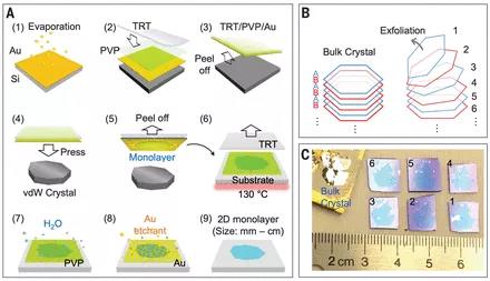
Fang Liu et al, Disassembling 2D van der Waals crystals into macroscopic monolayers and reassemblinginto artificial lattices, Science, 2020.
DOI: 10.1126 / science.aba1416
2. Science : Quantum anomalous Hall effect in MnBi 2 Te 4 , an intrinsic magnetic topological insulator
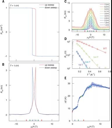
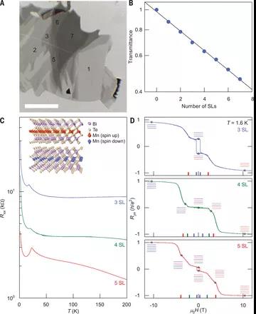
In magnetic topological insulators, the combination of non-flat band topology and magnetic order phase can produce strange states of matter, such as quantum anomaly (QAH) insulators and axon insulators. Zhang Yuanbo, Jing Wang of Fudan University, and Academician Chen Xianhui of the University of Science and Technology of China have studied quantum transmission in a MnBi 2 Te 4 sheet, which has an intrinsic magnetic order.
In this layered van der Waals crystal, the ferromagnetic layers are antiparallel coupled to each other; however, when the sample has an odd number of sample layers, the atomically thin MnBi 2 Te 4 becomes ferromagnetic. A zero-field QAH effect was observed in the five-layer and seven-layer samples of 1.4 K, and the external magnetic field aligned all layers by ferromagnetism to further increase the quantified temperature to 6.5 K. The discovered MnBi 2 Te 4 is an ideal place to further explore various topological phenomena.
Yujun Deng etal, Quantum anomalous Hall effect in intrinsic magnetic topological insulatorMnBi 2 Te 4 , Science, 2020.
DOI: 10.1126 / science.aax8156.
https://science.sciencemag.org/content/367/6480/895
3. Nature : High-resolution imaging of the boundary and growth structure of two-dimensional ice for the first time
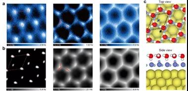
After nearly 100 years of research and exploration, 18 types of crystal phases (three-dimensional ice phases) of ice have been discovered so far. However, can ice exist independently and stably under the two-dimensional limit? This issue is highly controversial. In view of this, Jiang Ying , Peking University, Xu Limei, Wang Enge, Zeng Xiaocheng, University of Nebraska, Lincoln, etc. successfully grew a hydrophobic gold substrate (Au (111)) by precisely controlling the temperature and water pressure. A single crystal two-dimensional ice structure. This two-dimensional ice can completely cover the substrate.
The author further uses non-intrusive atomic force microscope imaging technology based on carbon monoxide needle tip modification to realize sub-molecular resolution imaging of two-dimensional ice by means of higher-order electrostatic forces, and determines its atomic structure in combination with theoretical calculations. The results show that this two-dimensional ice is formed by two layers of hexagonal ice stacked without rotation. The two layers are connected by hydrogen bonds. Each water molecule forms three hydrogen bonds with in-plane water molecules and forms with out-of-plane water molecules. One hydrogen bond, so all hydrogen bonds are saturated, the structure is very stable, and the interaction with the substrate is very weak. It is an intrinsic two-dimensional ice structure.
Runze Ma, Duanyun Cao, Chongqin Zhu, Ye Tian, Xiao Cheng Zeng *, Li-Mei Xu *, En-Ge Wang, * Ying Jiang *, et al. Atomic imaging of the edge structure and growth of atwo-dimensional hexagonal ice . Nature, 2019
DOI: 10.1038 / s41586-019-1853-4
https://www.nature.com/articles/s41586-019-1853-4
4. Nature: Reverse transformation of maze domain pattern in ferroelectric thin films
Phase separation is a cooperative process, and its dynamics provide the basis for the orderly formation of domain structures on the mesoscopic scale. Highly degenerate frozen state systems may experience rare and counterintuitive anti-symmetric failures. A study by the Y. Nahas team at the University of Arkansas found that after subcritical quenching, the non-equilibrium self-assembly of ferroelectric domains in Pb (Zr 0.4 Ti 0.6 ) O 3 ultrathin films can lead to the formation of labyrinths or labyrinth patterns with zigzag stripes. In addition, as the temperature rises, this highly degenerate labyrinth phase undergoes a reverse transition, thereby transforming into a less symmetric parallel-stripe domain structure before paraelectric start at high temperatures. It is found that the phase sequence can be attributed to the increase of the entropy of the domain wall, and the straightening and coarsening of the domain domain is mainly driven by the relaxation and diffusion of topological defects. The calculation model and experimental observation of inverse dipole transition in BiFeO 3 show that this phenomenon is universal in ferroelectric oxides. By implementing fundamental new design principles and topologically enhanced functions in ferroelectric thin films, many self-patterned states and their various topological defects can be used outside of the current field and domain wall-based technologies.
Inversetransition of labyrinthine domain patterns in ferroelectric thin films, Nature, 2020
https://www.nature.com/articles/s41586-019-1845-4
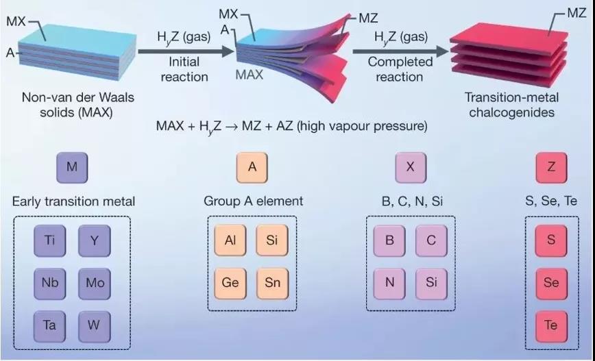
5. Nature : Large-scale preparation of ultra-stable TMC 2D materials
The practical application of two-dimensional materials, like many other emerging materials, is still constrained by the scale of materials. A key issue that has been faced in integrating single-layer TMCs into functional devices for a long time is that under environmental conditions, the stability of metal-phase single-layer TMCs often does not exceed one month. The research team of Yang Shubin from Beihang University and PuickelM. Ajayan and others from Rice University developed a new method for producing super stable two-dimensional materials in air through doping strategies . It can be stable under environmental conditions for more than one year. This method can directly convert non-Vandva solid materials to single-layer TMC, which is extremely universal, easy to operate, and low in cost, and is very suitable for industrial production. It greatly promotes the application of two-dimensional materials to the commercialization of the market.
Zhiguo Du et al. Conversion of non-vander Waalssolids to 2Dtransition-metal chalcogenides. Nature 2020, 577, 492-496.
https://www.nature.com/articles/s41586-019-1904-x2
6.Nature : Study on Synthesis and Properties of Single-layer Amorphous Carbon Materials
What is the difference between crystalline and amorphous materials? As early as 1932, Zachariasen proposed the Z-CRN model, which states that amorphous materials and their crystalline analogs contain the same bonding units, but these units form a continuous random network (Z-CRN) instead of a periodic structure. The other model, the competition model, considers that the internal atomic structure of amorphous materials and their crystalline analogs is not used at all, and there are nano-scale grains separated by grain boundaries in amorphous materials. For the past few decades, the Z-CRN model has prevailed, but the dispute between the two models has not been resolved. This is mainly because the atomic-scale characterization of amorphous materials has long been a problem. In view of this, the team of Professor Barbaros Özyilmaz and his collaborators at the National University of Singaporeanalyzed the structure of a single-layer amorphous two-dimensional carbon material at the atomic scale for the first time and found that it supports a competitive model more.
The researchers prepared a centimeter-level self-supporting single-layer amorphous two-dimensional carbon through a laser-assisted low-temperature CVD strategy, and found that its topology is different from graphene. Through accurate characterization by Raman spectroscopy and transmission electron microscopy, the researchers found that there is no long-range periodicity inside the material, and they observed that the bond lengths and bond angle sizes were different, and accompanied by a large number of five-membered rings, six-membered rings, seven-membered rings, Elementary ring, etc., the ring distribution does not follow the Z-CRN rules, and is more inclined to the competition model. Through theoretical calculations, the researchers found that this amorphous single-layer carbon material is not conductive, and the resistivity is close to that of BN nanomaterials obtained by CVD growth. Moreover, this material is extremely stable and has not broken, and will have potential applications in fields such as magnetic recording devices and flexible electronic devices.
Chee-TatToh et al. Synthesis and properties of free-standing monolayer amorphous carbon. Nature 2020, 577, 199--203.
https://www.nature.com/articles/s41586-019-1871-2
To date, most van der Waals heterojunction materials have been achieved by mechanical peeling or manual stacking methods. These methods are suitable for proof-of-concept during basic research, but they are not suitable for the development of practical application systems. As with all nanomaterials, to fully explore the potential of Van der Waals heterojunctions, we must first achieve the scaled and precisely controlled synthesis of van der Waals heterojunctions. This is a key challenge in this field for a long time and will face for a long time one. In view of this, Professor Duan Xidong from Hunan University and Professor Duan Fengfeng from UCLAhave reported the universal and controllable precise synthesis of two-dimensional van der Waals heterojunctions and constructed a high-current-density crystal diode for practical use. Application opens the way.
The authors first patterned on single-layer or double-layer s-TMD (such as WSe 2 , WS 2 , MoS 2 ) to produce nucleation sites with a periodic array. On this array, m-TMD can be selectively nucleated and grown to form a periodic m-TMD / s-TMD van der Waals heterojunction. This strategy is applicable to a variety of different materials and is not limited to a specific chemical composition or lattice structure. Can be used to process two-dimensional vdWH arrays between s-TMD and m-TMD without being affected by lattice differences. As a demonstration, the researchers used precise atoms, preferably close to the van der Waals attractive van der Waals interface manufacture a variety of 2D heterojunction comprises VSe 2 / WSe 2 , NITE 2 / WSe 2 , CoTe 2 / WSe 2 , NBTE 2 / WSe 2 , VS 2 / WSe 2 , VSe 2 / MoS 2 and VSe 2 / WS 2 .
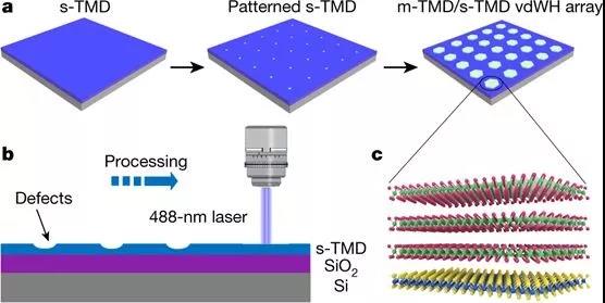
Jia Li et al. Generalsynthesis of two-dimensionalvan der Waals heterostructure arrays. Nature 2020.
https://www.nature.com/articles/s41586-020-2098-y
8. Nature : Optical observation of WSe 2 / WS 2 Mohr superlattice
The Moire fringe heterostructure of transition metal disulfide has a fairly strong light-matter interaction and a large spin-orbit coupling, which provides a new model system for studying related quantum phenomena. The problem is that it is difficult to directly observe the relevant insulation state in the system experimentally with traditional methods. In view of this, the FengWang team at the University of California, Berkeley reported a new strategy for optical observation of two-dimensional van der Waals heterojunction WSe 2 / WS 2 Mohr superlattices.
The researchers used a super-sensitive optical detection technology to find a Mott insulation state at a hole in each superlattice position, and even found insulation at 1/3 and 2/3 fills of each superlattice. Instead, researchers attribute this to the generalized Wigner crystals of the underlying lattice formation. Ultra-long spin relaxation lifetimes in the order of microseconds have been observed in the Mott insulation state, which are orders of magnitude longer than the lifetimes induced by charges. This study shows that Mohr superlattices other than graphene materials can also be very effective in exploring related physical phenomena.
mma C. Regan etal. Mottand generalized Wigner crystal states in WSe 2 / WS 2 moir��superlattices. Nature, 2020.
https://www.nature.com/articles/s41586-020-2092-4
9. Nature : Physical simulation of the Hubble model of the two-dimensional WSe 2 / WS 2 Mohr superlattice
In the 1960s, physicist John Hubbard proposed a simple theoretical model. The Hubble model can act as a quantum simulator in two-dimensional or three-dimensional physics to solve some crucial non-linear problems and reveal the physical principles of quantum particles with strong interactions. In view of this, KinFai Mak and Jie Shan of Cornell University reported the physical simulation of the Hubble model based on the 2D WSe 2 / WS 2 Mohr superlattice, and established a new type of research based on the Mohr superlattice. platform.
The researchers took the double-layer WSe 2 / WS 2 Mohr superlattice as the research object, and measured the charge and magnetism of the system by measuring the dependence of its optical response on the out-of-plane magnetic field and gate-tuned carrier density. The Mott insulation state with antiferromagnetic Curie�CWeiss phenomenon was observed in the semi-filled part of the first hole in the Mohr superlattice, which is consistent with the Hubbard model under strong interaction. Above half-filling, when the filling factor is close to 0.6, there may be a quantum phase transition from the antiferromagnetic state to the weak ferromagnetic state.

Yanhao Tang etal. Simulation of Hubbard model physics in WSe 2 / WS 2 moir�� superlattices. Nature, 2020.
https://www.nature.com/articles/s41586-020-2085-3
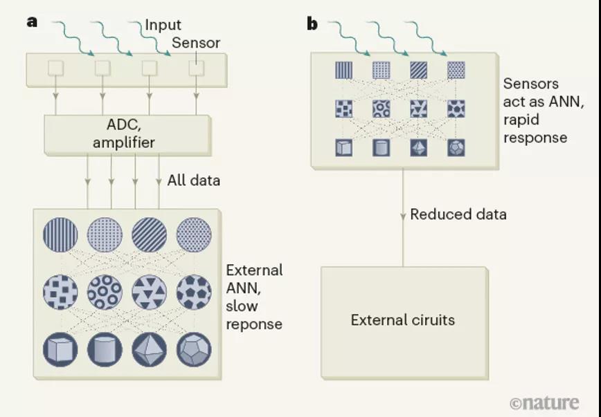
10.Nature : Two-dimensional materials make ultra-fast image recognition sensors possible!
Whether in autonomous driving or emerging technologies such as face recognition, ultra-fast visual image sensing technology has become a key component of intelligent systems. The problem is that the ultra-fast conversion of optical images into the electrical signal domain is still one of the bottlenecks in the field. With artificial neural network technology that mimics the structure of the human eye, it has great potential in enhancing image contrast, noise reduction or data acquisition, and is expected to make breakthroughs in this field. In view of this, Lukas Mennel and Thomas Mueller from the University of Technology in Vienna, Austria, and others reported the latest results of ultra-fast image recognition based on two-dimensional materials. Professor Yang Chai of the Hong Kong Polytechnic University was invited to comment on this in Nature and made a prospect.
Researchers have demonstrated that the image sensor itself can form an artificial neural network while sensing and processing optical images without delay. Based on the WSe 2 two-dimensional semiconductor as a photosensitive material, a reconfigurable photodiode array was constructed, which showed strong light-matter interaction and excellent photoelectric properties. It implements supervised and unsupervised learning, and trains sensors to classify and encode images projected on the chip optically, with a processing capacity of 20 million bins per second.
1.Lukas Mennelet al. Ultrafast machine vision with 2D material neural networkimage sensors.Nature 2002.
https://www.nature.com/articles/s41586-020-2038-x
2. Yang Chai et al. In-sensor computing for machinevision. Nature 2002.
https://www.nature.com/articles/d41586-020-00592-6
11. Nature : New strategy for growing wafer-level single-layer hexagonal boron nitride single crystals
In integrated circuits, ultrathin two-dimensional semiconductor materials offer great potential for extending Moore��s Law. One of the key issues is how to avoid the formation of charge scattering and trap sites between adjacent dielectrics. The hexagonal boron nitride (hBN) insulating van der Waals layer provides an excellent interfacial dielectric, effectively reducing the scattering of charge. Single crystal hexagonal boron nitride is usually grown on the surface of molten gold or on bulk copper foil. However, the high cost of molten gold, cross-contamination, and potential problems with process control and scalability are not welcomed by companies. Copper foil may be suitable for roll-to-roll processes, but is unlikely to be compatible with advanced microelectronics manufacturing on wafers. Therefore, how to reliably grow single crystal hBN directly on a wafer is one of the key technologies in the semiconductor field. In view of this, Lain-Jong Li, Wen-Hao Chang, and Boris I. Yakobson et al. Reported a new strategy for growing wafer-level single-layer hexagonal boron nitride single crystals on the surface of Cu (111) single crystals. The application of dimensional materials in the field of electronic devices has laid the foundation.
Using a two-inch c-plane sapphire wafer as the substrate, the researchers successfully prepared a single crystal hBN single layer by epitaxial growth on a Cu (111) single crystal thin film. First-principles calculations indicate that the Cu (111) step of hBN lateral docking can enhance epitaxial growth, thereby ensuring the unidirectionality of the hBN monolayer. Using single crystal hBN as the interface layer between MoS 2 and HfO 2 effectively improves the electrical performance of the transistor.
Tse-AnChen etal. Wafer-scale single-crystal hexagonal boron nitride monolayers on Cu (111) .Nature 2020.
https://www.nature.com/articles/s41586-020-2009-2
Source: Nanoman

| Reminder: Beijing Beike New Material Technology Co., Ltd. supplies products only for scientific research, not for humans |
| All rights reserved © 2019 beijing beike new material Technology Co., Ltd ��ICP��16054715-2�� |
