
hotline��
17715390137
Tel/Wechat��
18101240246 (Technology)
0512-68565571
Email��mxenes@163.com ��Sales Engineer��bkxc.bonnie@gmail.com
Scan the code to follow or search the official account on WeChat:
2D Materials Fronrier After paying attention,
click on the lower right corner to contact us,
Enter enterprise WeChat.
Professional Services Online


| Although graphene in itself has been dubbed the ��magic�� material, if it is to be used for practical applications it has to integrated with the other components of possible devices. For instance, to exploit its amazing electron conduction properties, you still need to connect it to the rest of the circuit with contacts, which are typically made out of metal. | |
| Understanding how metals interact �C chemically and structurally �C with graphene is therefore quite important and researchers have published a number of studies on the subject (see for instance this recent paper in Nano Letters: "Metal-Graphene Interaction Studied via Atomic Resolution Scanning Transmission Electron Microscopy"). | |
| In a quite unexpected discovery resulting from these observations, researchers have now found that graphene undergoes a self-repairing process to close holes that are caused by metal atoms. Reporting their findings in the July 5, 2012 online edition of Nano Letters ("Graphene Reknits Its Holes"), a team from The University of Manchester and SuperSTEM Laboratory, both in the UK, has shown that nanoscale holes (perhaps a 100 atoms missing or so), etched under an electron beam at room temperature in single-layer graphene sheets as a result of their interaction with metal impurities, heal spontaneously by filling up with either nonhexagon, graphene-like, or perfect hexagon 2D structures. In the process, loose carbon atoms will migrate over the surface of graphene spontaneously and will attach to the edges of the hole, filling it up quite quickly. The scientists were actually able to capture this mechanism in a series of images showing almost atom-by-atom how this hole filling process takes place. | |
| "One of our earlier findings ("Direct Experimental Evidence of Metal-Mediated Etching of Suspended Graphene") was that in specific conditions, metal atoms �C except for gold �C seem to mediate a remarkable etching process: they help create holes in graphene," Quentin Ramasse, Scientific Director at SuperSTEM, tells Nanowerk. "In simple terms, put some metal near the graphene sheet, add some energy, most likely some oxygen as well, and the metals atoms will catalyze a bond breaking reaction. The carbon-carbon bonds break, a hole forms, more metal atoms are attracted to that hole and help breaking more bonds, and the hole keeps getting bigger until the reservoir of metal atoms is exhausted." | |
|
|
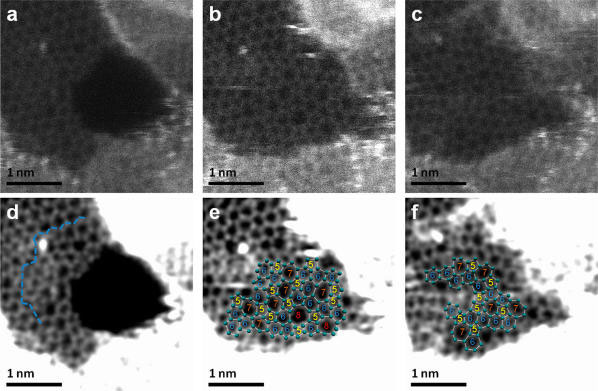
| Atomic resolution Z-contrast images illustrating the hole filling process in suspended graphene. (a) A hole created at the border of the hydrocarbon contamination starts to ��mend�� with C polygons. (b) Complete reconstruction with incorporation of 5-7 rings and two 5-8 rings, and (c) redistribution of defects in the ��mended�� region, by 5-7 rings. Images (d-f) are processed versions of (a-c). A maximum entropy deconvolution algorithm was used and the contrast was optimized to visualize the carbon atoms. The carbon atom positions are highlighted by light green dots and polygons numbered according to the number of atoms in the rings. (Reprinted with permission from American Chemical Society) | |
| Ramasse points out that this process does not take place without the metal atoms being present: "Our instruments allow us to observe graphene atom by atom for extremely long periods of time without any damage to the material." | |
| The team �C which included Recep Zan, Ursel Bangert and Konstantin S. Novoselov, who shared a Nobel prize as graphene��s co-discoverer �C were studying this phenomenon when they realized that some of the holes that had been created through the process described above were mending themselves, filling up with new carbon atoms that most likely came from a nearby ��reservoir�� of carbon �C essentially a patch of carbon-based contamination sitting not too far away from the hole. | |
| "The fact that the hole was repairing itself is remarkable enough" says Ramasse. "Having said that, we know that holes/edges in graphene are not energetically favorable and loose carbon atoms can diffuse very fast on the surface of graphene, so it is not totally unexpected: if there is no more reason for the hole to be enlarged, in other words, if the etching process has stopped, then the material will try to compensate for this unstable hole that has been created and an easy way to do so is to fill it up." | |
| "What was more remarkable" he continues, "was the fact that the hole did not necessarily fill up with perfect graphene lattice, but with C atoms somewhat randomly bonded to other carbon atoms, not in the usual honeycomb 6-fold pattern but in 5-, 6-, 7- or even 8-member rings without any obvious medium- or long-range order. In other words, what we observed is a 2-dimensional ��quasi��-amorphous structure." | |
| The balance between the etching and filling mechanisms may be the difference between a working device and a proof of concept without any real application. Therefore, it may be somewhat re-assuring that if holes are created by putting metals and graphene in close proximity, this system has a tendency to self repair. However, the team��s observations are very much on the fundamental side of things: they were looking at a model system, not a real metal contact in a graphene-based device. | |
| From a more abstract point of view, the observation of two-dimensional amorphous structures is fascinating. "For obvious reasons, it is extremely hard to say anything about amorphous materials on the atomic level" says Ramasse. "There is no order, no repeat units, so how does one go about describing how atoms bond with one-another? Seeing a 2-dimensional version of it as we did, means that we can actually study atom by atom those quasi-random structures, and get a lot of insights about how these materials might look in the full 3 dimensions." | |
| The foundation of all this recent nanoscale work on graphene and other materials is the fact that, thanks to recent technological advances, scientists now have tools to observe materials one atom at a time, including sensitive ones such as graphene which is only one atom thick. | |
| An extremely powerful microscope used by the Manchester team (an advanced electron microscope built by a small U.S. company called Nion) allows the capture of images of graphene where every single atom in the structure is resolved, without damaging the material observed. It allows the researchers to tell what those atoms are, where they sit in the structure, distinguish between impurity atoms �C oxygen, silicon or metal impurities for instance �C and to a certain extent tell how they bond to their neighbors. | |
| "From a materials science point of view, this is an extremely exciting time, because these are exactly the questions we need to answer to understand where specific materials properties come from, and it is in turn invaluable when designing materials for the future," says Ramasse. "This approach is of course very relevant to graphene: being only one atom thin, you need these capabilities to study it." | |
| A distinct possibility arising from this research, albeit somewhat further afield, is the ability for new ways to sculpt graphene or two-dimensional carbon sheets. | |
| "People have shown that depending on their shapes, graphene nanostructures, nanoribbons for instance, have even more exotic and remarkable properties," says Ramasse. "So if we have a way of controlling the etching process, drilling through graphene in a controlled fashion to sculpt it at the atomic level, but also to grow it back in new shapes or to fill up holes that were made a little too big, this adds a lot of flexibility to our nanotechnology toolbox." | |
|
He cautions, though, that graphene has seen so much media exposure that the main challenge for researchers in the field is to live up to the expectations they have created. "Those amazing properties of the material must be utilized in ��real-world�� practical applications, in new, more powerful devices that were not possible without graphene. While graphene-based devices are starting to show up here and there, there is still a long way to go before it enters our every day life �C probably because there is still a lot we don��t understand about it."
Source: Nanowerk |

| Reminder: Beijing Beike New Material Technology Co., Ltd. supplies products only for scientific research, not for humans |
| All rights reserved © 2019 beijing beike new material Technology Co., Ltd ��ICP��16054715-2�� |
