source��beike new materialViews��8965time��2020-08-10 QQ Academic Group: 1092348845
Graphene is the name of a thick-atom honeycomb sheet of carbon atoms. It is the basis of other graphite materials (since the typical carbon atom diameter is about 0.33 nanometers, there are about 3 million layers of graphene in 1 millimeter of graphite).
Harder than diamond, but more elastic than rubber; harder than steel, but lighter than aluminum. Graphene is the strongest known material.
From a perspective: If a cling film (such as a kitchen cling film) has the same strength as the original single-layer graphene, a 2000 kg weight or the force applied by a large car is required to pierce it with a pencil.
Graphene also has other surprising properties: its high electron mobility is 100 times faster than silicon; its thermal conductivity is twice that of diamond. Its conductivity is 13 times better than copper; it absorbs only 2.3% of the reflected light; it is impermeable, so even the smallest atom (helium) cannot pass through a single-layer graphene sheet without defects. Its high surface area is 2630 square meters per gram, which means less than 3 grams, you can cover the entire football field (well, you actually need 6 grams, because 2630 m 2 / g is a graphene sheet with a surface area on both sides).
Graphene is a basic component of other graphite materials. It also represents a class of new materials that are conceptually only one atom thick, the so-called two-dimensional (2D) materials (the reason they are called 2D materials because they only extend in two dimensions: length and width; because of this If the material is only one atom thick, the third dimension (height) is regarded as zero).
For manufacturing a graphene van der Waals heterostructures of mixed sizes are also very attractive, the heterostructure can be produced by graphene nanoparticles or quantum dots 0D, 1D nanostructures (e.g., nanowires or carbon nanotubes) or 3D bulk material To achieve hybridization.
Graphene graph
We have summarized a chart summarizing the key characteristics, facts and application areas of graphene. Click to enlarge and embed and share at any time.
Learn about graphene (click the image to enlarge). Download as PDF (13.9 MB). Share this picture on your website:
The extraordinary properties of graphene originate from the 2p orbit, which forms ��-state bands, which are delocalized on the carbon sheet constituting graphene.
Graphene is one of the most promising nanomaterials due to its unique combination of outstanding properties : it is not only the thinnest material, but also the strongest material. Its thermal conductivity is superior to all other materials; it is a great conductor of electricity. It is optically transparent, but so dense that it is gas-impermeable, even the smallest gas atom, helium, cannot pass through.
These amazing properties and their versatility make graphene suitable for a wide range of applications from electronics to optics, sensors and biological devices.
Graphene research has developed into a vast field, and now about 10,000 scientific papers covering a wide range of topics are published every year.
Graphene discovery
Carbon comes in many forms (so-called allotropes ), from graphite in pencil to the most expensive diamond in the world. In 1980, we only knew three basic forms of carbon, namely diamond, graphite and amorphous carbon. Then, fullerenes and carbon nanotubes were discovered. In 2004, graphene joined the club.
In the two physicists at the University of Manchester, Jim Andre (Andre Geim) and Konstantinŵ�������(Konstantin Novoselov) in 2004 and in first discovered before graphene (they in 2010 won the Nobel Prize ), Scientists argue that strictly speaking, 2D crystal materials are thermodynamically unstable and cannot exist.
In the initial experiment, Geim and Novoselov extracted graphene from graphite found in a common pencil. They used conventional tape to manage to obtain carbon flakes that were only one atom thick. Mechanical peeling is the simplest method of preparation, and surprisingly the method that makes standalone graphene a reality.
Watch a wonderful introduction video about graphene
Graphene manufacturing method
The quality of graphene plays a crucial role, because there are defects, impurities, grain boundaries, multiple regions, disordered structure, and wrinkles in the graphene sheet, which will adversely affect its electronic and optical properties.
In electronic applications, the main bottleneck is the need for large-size samples, which is only possible in the case of CVD processes, but it is difficult to produce high-quality single-crystal graphene films that have high conductivity and Thermal conductivity, and has excellent electrical conductivity. Optical transparency.
Another issue that needs attention when synthesizing graphene by conventional methods is the use of toxic chemicals. These methods usually produce hazardous waste and toxic gases. Therefore, it is necessary to develop a green method for producing graphene by following an environmentally friendly method.
Graphene preparation methods should also allow in- situ manufacturing and integration of graphene-based devices with complex architectures , which can eliminate multi-step and laborious manufacturing methods at lower production costs (read more: " Mass production: analysis of global patents " ).
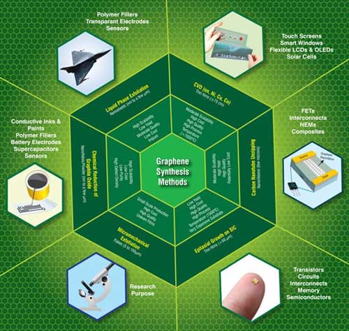
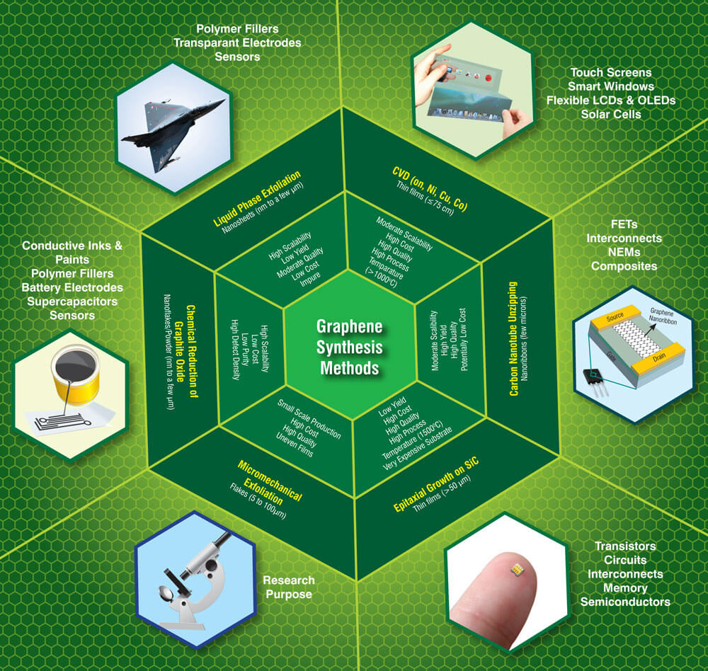
At present, the most commonly used technologies that can be used to produce graphene are shown in the following figure, including micromechanical cutting, chemical vapor deposition, epitaxial growth on SiC substrates, chemical reduction of sheet-like graphene oxide, and liquid phase exfoliation (LPE) of graphite And the decompression of graphene. Carbon nanotubes.
However, each of these methods has its own advantages and limitations, depending on its target application. In order to overcome these obstacles to the commercialization of graphene, researchers from various R & D institutions, universities and companies around the world are working together to develop new methods for mass production of low-cost and high-quality graphene through simple, environmentally friendly. Friendly method.
Researchers have managed to produce large single-crystal graphene films over a foot long on almost any plane , which is a step towards commercialization.
However, a big caveat here: global graphene production seems to be plagued by serious quality problems, and there does not seem to be high-quality graphene as defined by ISO on the market. Read more: Beware of fake graphene .
This schematic diagram shows the conventional methods commonly used to synthesize graphene and their key features, as well as current and future applications. (Photo: CKMNT) (click on the image to enlarge)
One of the reasons why nanotechnology researchers dedicated to molecular electronics are so excited about graphene is its electronic properties-it is one of the best electrical conductors on earth. The unique atomic arrangement of carbon atoms in graphene makes it easy for electrons to travel at extremely high speeds without significant scattering opportunities, thereby saving valuable energy that is usually lost in other conductors.
Scientists have found that even at a nominal carrier concentration of zero, graphene still has the ability to conduct electricity because electrons do not seem to slow down or locate. The electrons moving around the carbon atoms interact with the periodic potential of graphene��s honeycomb lattice, creating new quasiparticles that lose mass or rest mass (so-called massless Dirac fermions ). This means that graphene will never stop conducting electricity. They also found that they travel much faster than electrons in other semiconductors.
Mechanical behavior
Graphene��s impressive inherent mechanical properties, its stiffness, strength and toughness, are one of the reasons that make graphene stand out as a reinforcing agent in individual materials and composites. They are made SP 2 bond due to stability, SP 2 bond form a hexagonal lattice plane and resists the various modification.
A detailed discussion on the mechanical properties of graphene and graphene-based nanocomposites can be found in this review article .
rigidity
The breaking force obtained by experiment and simulation is almost the same, and the experimental value of the second-order elastic stiffness is equal to 340 �� 50 N m -1 . Assuming an effective thickness of 0.335 nm, this value corresponds to a Young��s modulus of 1.0 �� 0.1 TPa.
strength
The defect-free single-layer graphene is considered to be the strongest material ever tested , with a strength of 42 N m -1 and an inherent strength of 130 GPa.
toughness
Fracture toughness is related engineering properties, is one of the most important mechanical properties of graphene, and a critical stress intensity factor of 4.0 �� 0.6 MPa was measured .
Research teams around the world are working on the development of industrially manufactured graphene sheets that have high strength and toughness in all sheet directions and can be used for various purposes, such as for vehicles, optoelectronics, and nerve implantation It was graphene-based composites .
Examples of newly developed consumer products that utilize the mechanical properties of graphene are Momo Evo graphene motorcycle helmets developed by Momodesign in Italy and Italian Institute of Technology (IIT) .
This is the first carbon fiber helmet infused with graphene. The helmet uses the material��s thin, strong, conductive, flexible and lightweight characteristics to create a helmet that absorbs and dissipates impact better than ordinary helmets. It can also dissipate heat more efficiently, so the temperature is lower.
Another example is the Dassi Interceptor ™ graphene bicycle -the world��s first graphene bicycle. Reinforcing carbon fibers with graphene can make stronger, lighter, thinner tubes than ordinary carbon. This means that the aero-shaped frame does not sacrifice any usual weight. Thanks to its graphene-reinforced frame, the weight of this bicycle has been reduced by 30%, but its strength and super stiffness have doubled.
The researchers also found that there is a critical and unexpected relationship between the chemical / structural defects of graphene as the electrode��s host material and its ability to inhibit dendrite growth. Dendritic filaments are deposited on the electrode and can penetrate the barrier between the two halves of the electrode. May cause battery short circuit, overheating and fire ("non- defective graphene may solve the dendrite problem of lithium metal batteries ").
These examples highlight the impact of graphene on four major energy-related areas: solar cells, supercapacitors, graphene batteries, and fuel cells.
Due to its excellent electron transport properties and extremely high carrier mobility, graphene and other direct bandgap monolayer materials (such as transition metal carbon disulfide (TMDC) and black phosphorus) show great potential for low cost , Flexible and efficient photovoltaic equipment. They are the most promising materials for advanced solar cells .
The authors point out, however, that before graphene-based nanomaterials and devices are widely used in commercial applications, two important issues must be solved: one is the preparation of graphene-based nanomaterials with a clear structure, and the other is the controlled preparation of graphene. These materials become functional devices.
Sensor application
Functionalized graphene has extraordinary prospects in biological and chemical sensors. Researchers have shown that the unique 2D structure of graphene oxide (GO) combined with super-permeability to water molecules causes the sensing device to operate at an unprecedented speed ( "Ultra-fast graphene sensors can monitor your Breathe " ).
Scientists have discovered that chemical vapors can change the noise spectrum of graphene transistors, allowing them to selectively gas-sensing multiple vapors through a device made of virgin graphene �C without the need to functionalize the graphene surface ( "use Raw graphene is used for selective gas sensing " ).
Graphene has a unique combination of properties and is very suitable for the next generation of electronic products, including mechanical flexibility, high conductivity and chemical stability. Combining it with inkjet printing, you will get an inexpensive and scalable way to take advantage of these features in real-world technology ( "Inkjet printing of graphene for flexible electronic devices" ).
Transistors and memory
The most promising applications of graphene are in the electronics field (as transistors and interconnects), detectors (as sensor elements) and thermal management (as lateral heat sinks). The first graphene field effect transistor (FET) with both bottom and top gates has been demonstrated. At the same time, for any transistor that can be used in analog communication or digital applications, the level of electronic low-frequency noise must be reduced to an acceptable level ( "graphene transistors can work without generating a lot of noise" ).
Graphene-based transistors are considered potential successors to certain silicon components currently in use. Since electrons can move through graphene faster than through silicon, the material has the potential to achieve terahertz calculations.
In the final nanoscale transistors (called ballistic transistors ), electrons can avoid collisions, that is, there is almost no obstruction to the passage of current. Ballistic conduction will make the switchgear extremely fast. Graphene has the potential to enable bulletproof transistors at room temperature.
Experiments have demonstrated the benefits of graphene as a flash memory platform , indicating that the inherent characteristics of graphene may exceed the performance of current flash memory technology.
Flexible, retractable and foldable electronics
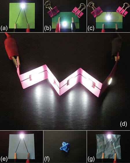
Flexible electronic products rely on flexible substrates, while true foldable electronic products require foldable substrates with very stable conductors that can withstand folds (ie, creases on the edges of the substrate at the fold point, even after unfolding Will still deform).
This means that in addition to a foldable substrate like paper, the conductor deposited on the substrate also needs to be foldable. To this end, the researchers showed a manufacturing process of foldable graphene circuits based on paper substrates .
Photos of the application. a, b, c) Running LED chips with graphene circuits on paper substrates at -180 �� folding and 180 �� folding. d) LED chip array on the three-dimensional circuit board, including negative angle folding and positive angle folding. e, f, g) Before and after wrinkling, the LED chip on the paper-based circuit board operates. (Reprinted with permission from Wiley-VCH Verlag)
Graphene��s excellent electrical conductivity, strength and elasticity also make it a promising choice for stretchable electronic products-a technology aimed at producing circuits on flexible plastic substrates, which can be used in flexible solar cells or robot-like Artificial skin.
Scientists have devised a chemical vapor deposition (CVD) method that can transform graphene sheets into a porous three-dimensional foam with extremely high electrical conductivity. By penetrating the foam with a silicone-based polymer, researchers can manufacture a twist, bending and stretching the composite without damaging the electrical or mechanical properties ( "Graphene: Electronic products stretchable Bubble " ).
Photodetector
Researchers have proven that graphene can be used in telecommunications applications, and its weak and versatile optical response may translate into advantages for ultrafast photonic applications. They also found that graphene may be used as a saturated light absorber, and its optical response ranges from ultraviolet, visible, and infrared to terahertz ( "the rise of graphene in ultrafast photonics" ).
There is a very strong research interest in the use of graphene in optoelectronics. Graphene-based photodetectors have been implemented before, and graphene has been proven for high-bandwidth photoelectric detection in an optical data link of 10 GBit / s ( "Graphene photodetectors for high-speed optical communication" ) Applicability .
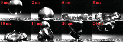
Coating objects with graphene can achieve different purposes. For example, researchers have now shown that graphene sheets can be used to make superhydrophobic coatings that exhibit stable superhydrophobicity under both static and dynamic (droplet impact) conditions, resulting in extremely strong water-repellent structures .
Snapshots of water droplets can affect the surface of Teflon-coated graphene foam. The impact velocity before the droplet hits the surface is about 76 cm / sec. The snapshot sequence shows the history of the deformation time of the droplet after impact. The droplet spreads, then retracts and successfully bounces off the surface. For Teflon-coated foams, the recovery factor (the ratio of droplet impact velocity to jet velocity) is about 0.37. (Reprinted with permission from Wiley-VCH Verlag)
Graphene is also the thinnest coating in the world to protect metals from corrosion. It has been found that graphene, whether made directly on copper or nickel, or transferred to another metal, can provide corrosion protection .
The researchers demonstrated the use of graphene as a transparent conductive coating for photonic devices, and showed that its high transparency and low resistivity make this two-dimensional crystal very suitable for electrodes in liquid crystal devices (LCD) .
Another novel coating application that is useful to researchers is to make polymer AFM probes covered with a single layer of graphene to improve the performance of AFM probes .
Other uses
loudspeaker
The extraordinary electrical and mechanical properties of graphene have been utilized to create very effective electrical / acoustic transducers. This experimental graphene speaker does not have any optimized acoustic design, is simple to manufacture, and is already comparable to or even better than commercial speakers of similar size, and has much lower power consumption.
The Artisanphonics CB-01Nanene® headphones feature a diaphragm membrane made with graphene in each earpiece, so it is very thin but has the same strength and durability as a conventional membrane. However, due to its flexibility, it can be controlled better, thereby enhancing treble and bass.
Over the decades of building artificial muscles, it has been studied whether many materials are suitable for actuator applications (driving is the ability of materials to change size reversibly under various stimuli). In addition to artificial muscles, potential applications include micro-electromechanical systems (MEMS), bionic micro- and nano-robots, and micro-fluidic devices. In experiments, scientists have shown that graphene nanoribbons can provide a driving effect .
Due to the rapid increase in power density in electronic devices, managing the resulting heat has become one of the most critical issues in computer and semiconductor design. In fact, heat dissipation has become a basic problem for nano-scale electron transmission.
This is where graphene appears �C its thermal conductivity is better than any other known material (