
hotline:
17715390137
Tel/Wechat:
18101240246 (Technology)
0512-68565571
Email:mxenes@163.com (Sales Engineer)bkxc.bonnie@gmail.com
Scan the code to follow or search the official account on WeChat:
2D Materials Fronrier After paying attention,
click on the lower right corner to contact us,
Enter enterprise WeChat.
Professional Services Online


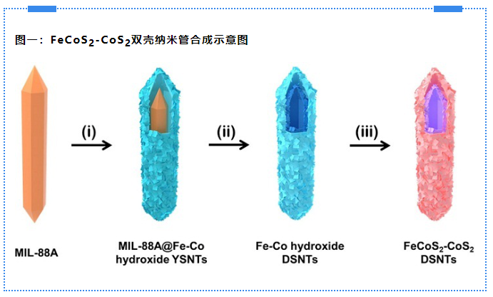
Angewandte Chemie International Edition FeCoS2-CoS2 double-layer nanotubes have enhanced photocatalytic reduction of CO2 performance
Metal sulfide semiconductors have great potential in the photocatalytic reduction of CO2 due to their suitable energy band structure, excellent redox activity, and adjustable electrical and optical properties. Lou Xiongwen’s research group at Nanyang Technological University in Singapore reported a simple metal-organic framework (MOFs)-assisted synthesis method to prepare hierarchical FeCoS2-CoS2 double-shell nanotubes (DSNTs), in which both shells are made of 2D nanosheets The unit is assembled. This synthesis strategy uses a two-step cation exchange reaction to precisely integrate two metal sulfides into a double-shell tubular heterostructure, and both shells are assembled from ultra-thin 2D nanosheets. Benefiting from its unique structure and composition, FeCoS2-CoS2 hybrids can reduce the volume of photoexcited charge carriers to the surface diffusion length to promote their separation. This hybrid structure can expose abundant active sites to enhance CO2 adsorption and surface-dependent redox reactions, and more effectively collect incident sunlight through complex internal light scattering. These layered FeCoS2-CoS2 double-shell nanotubes show excellent activity and high stability for photosensitive deoxygenation CO2 reduction, and the CO generation rate is as high as 28.1 mmolh-1 (per 0.5 mg catalyst). [1] Related results were published in Angewandte Chemie International Edition with the title "Formation of Hierarchical FeCoS2-CoS2 Double-Shelled Nanotubes with Enhanced Performance for Photocatalytic Reduction of CO2".
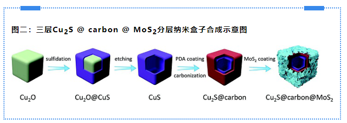
2. Angewandte Chemie International Edition reasonably designed three-layer Cu2S @ Carbon @ MoS2 multilayer nano box for efficient sodium storage
Metal sulfides have received extensive attention from researchers due to their diverse composition and good electrochemical properties. Among them, the composite metal sulfide exhibits high-efficiency sodium storage performance due to the synergy between the components. The Lou Xiongwen research group of Nanyang Technological University in Singapore reported on a carefully designed and synthesized layered nano box with Cu2S@Carbon@MoS2 as the anode material for sodium ion batteries. The synthesis process uses Cu2O nanocubes as a template to obtain a hollow CuS structure through vulcanization and etching reactions; after PDA coating and subsequent carbonization reaction, a nitrogen-doped carbon-coated Cu2S hollow structure (Cu2S@Carbon) is obtained; further use In the solvothermal reaction, a layer of MoS2 nanosheets is grown on the surface of Cu2S@Carbon, resulting in a three-layer hollow structure of Cu2S@Carbon@MoS2. This design shortens the electron/sodium ion diffusion path, adapts to the volume change of the electrode during the cycle, enhances the conductivity of the hybrid, and provides abundant active sites for sodium absorption. With these advantages, these three-layer Cu2S@Carbon@MoS2 layered nano-boxes exhibit excellent electrochemical performance in terms of good rate capability and stable cycle life. This research provides a new strategy for preparing complex mixed metal sulfide anode materials with high-performance hierarchical structure, and provides new ideas for the development and application of sodium ion batteries and the synthesis of materials with complex hierarchical structures. [2] Relevant results were published in Angewandte Chemie International Edition with the title "Rationally Designed Three-Layered Cu2S@Carbon@MoS2 Hierarchical Nanoboxes for Efficient Sodium Storage".
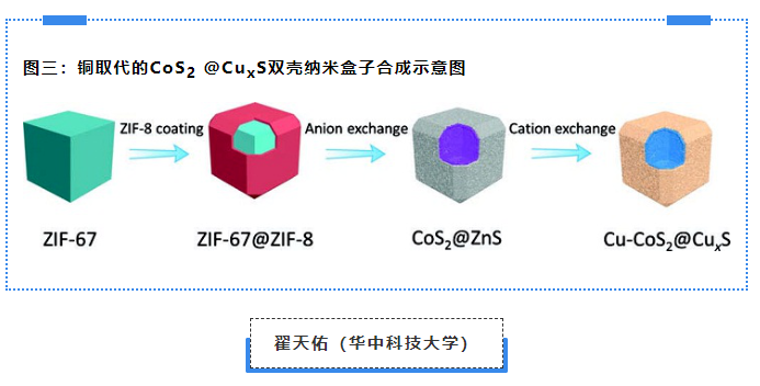
3. Angewandte Chemie International Edition synthesizes copper-substituted CoS2@CuxS double-shell nanoboxes for efficient sodium storage through sequential ion exchange
The layered hollow nanostructures assembled from nanoscale components show enhanced sodium storage characteristics and can reduce the diffusion paths of sodium ions and electrons, and the hollow structure can adapt to the strain during the electrochemical reaction. Due to the synergy of each component, the construction of a hybrid system structure of electrode materials has been proven to be an effective strategy to improve sodium storage performance. The research group of Nanyang Technological University Lou Xiongwen reported the synthesis of integrated nanostructures (Cu-CoS2@CuxS DSNBs) composed of copper-substituted CoS2@CuxS double-shell nanoboxes through a templating strategy based on metal-organic frameworks (MOFs). Using ZIF-67 nanocubes as raw materials, ZIF-67@ZIF 8 polyhedrons were synthesized by epitaxial growth; the obtained ZIF-67@ZIF-8 polyhedrons were converted into Cu-CoS2 through sequential ion exchange reactions with S2- and Cu2+ @CuxS DSNBs. Cu-CoS2@CuxS DSNBs have a unique shell structure and complex composition. They have high capacity (535 mA h g-1 at 0.1 A g-1) and high magnification (333 mA h g at 5 A g-1). -1) and long cycle (76% capacity retention rate in 300 cycles) showing excellent sodium storage performance. This research provides inspiration for the design and manufacture of complex heterostructures for various applications, and provides a new idea for the development of sodium ion batteries. [3] Relevant results were published in Angewandte Chemie International Edition under the title "Synthesis of Copper-Substituted CoS2@CuxS Double-Shelled Nanoboxes by Sequential Ion Exchange for Efficient Sodium Storage".
Di Tianyou (Huazhong University of Science and Technology)
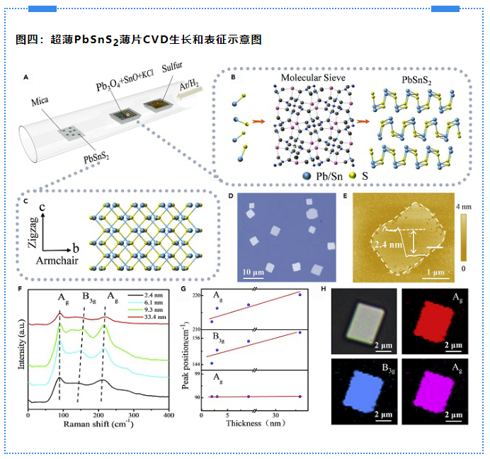
4. Matter grows ultra-thin ternary PbSnS2 sheets for highly anisotropic photovoltaics
Two-dimensional (2D) ternary materials, as a new member of the 2D material family, have received widespread attention due to their additional degrees of freedom from multiple element compounds. This variable stoichiometric ratio in two-dimensional ternary materials will have a significant impact on the band structure, phonon vibration, lattice symmetry, and carrier transport. Huazhong University of Science and Technology Zhai Tianyou’s research group synthesized ultra-thin 2D PbSnS2 flakes by salt and molecular sieve-assisted chemical vapor deposition (CVD), whose thickness can be as thin as 2.4 nm. The addition of butadiene molecular sieve reduced the melting point and the metal precursor respectively. Source steam evenly distributed in the reaction system. The phototransistor based on 2D PbSnS2 sheet exhibited huge anisotropic electronic devices (hole mobility: μarmchair / μzigzag = 1.78) and photoelectric devices (response: Rzigzag / Rarchair = 1.25), and both armchair and zigzag directions showed Fast response speed of about a few milliseconds. The research used salt and molecular sieves in the CVD process for the successful synthesis of ultra-thin PbSnS2 flakes may provide a new platform for the design of other 2D ternary materials. [4] Related results were published in Matter under the title of "Growth of Ultrathin Ternary Teallite (PbSnS2) Flakes for Highly Anisotropic Optoelectronics".
5. Adv. Funct. Mater. Salt-assisted growth of P-type Cu9S5 nanosheets for high-responsive P-N heterojunction photodetectors
The p-n junction based on two-dimensional (2D) van der Waals heterostructures is one of the most promising alternatives in next-generation electronics and optoelectronics. By choosing different 2D transition metal dihalides (TMDC), the p-n junction has a customized energy band arrangement and has excellent photodetector performance. A p-n diode operating under a reverse bias generally has a higher detection rate due to suppression of dark current, but has a lower responsiveness due to low quantum efficiency. The larger built-in electric field in the depletion layer can improve the quantum efficiency by reducing the recombination of charge carriers. The research group of Huazhong University of Science and Technology Tianyou Zhai synthesized a new type of p-type semiconductor Cu9S5 with direct band gap and high light absorption coefficient by salt-assisted chemical vapor deposition (CVD) method. According to the Anderson heterojunction model, the high density of holes in Cu9S5 endows the p-n junction Cu9S5/MoS2 with a strong built-in electric field. Due to the effective charge separation, the Cu9S5/MoS2 p-n heterojunction has a lower dark current when reverse biased, and a higher light response under illumination. The Cu9S5/MoS2 photodetector showed good light detection of 1.6×10¹² Jones and light responsiveness of 76 A W-1 under light. This study shows that the two-dimensional Cu9S5 nanosheet is a novel p-type semiconductor with good prospects in optoelectronic applications, which may further pave the way for the introduction of Cu2-xS (0
6. Adv. Funct. Mater. Sub-millimeter single layer p-type H phase VS2
Compared with metal T-phase structure, 2D H-phase vanadium disulfide (VS2) is expected to exhibit adjustable semiconductor performance, which is expected to play a role in future electronic applications. Due to the polymorphic form of vanadium sulfide and the thermodynamic instability of H-phase VS2, the two-dimensional H-phase VS2 nanostructure has not been realized in experiments. By introducing a molten salt-mediated precursor system and an epitaxial mica growth platform, Zhai Tianyou’s research group at Huazhong University of Science and Technology constructed a unique growth environment to prepare an H-phase VS2 monolayer with a lateral dimension of up to 250 mm, and made the 2D H of VS2 The phase structure is evolved. Through spherical aberration corrected scanning transmission electron microscope and second harmonic generation characterization, the honeycomb structure of H-phase VS2 with inversion symmetry was confirmed, and the phase structure was found to be in an ultra-stable state up to 500 K. Field-effect device research further proves the p-type semiconductor properties of 2D H-phase VS2. This research introduces a new phase stable 2D transition metal sulfide material, laying the foundation for the development of electronic devices. [6] The related results are titled "Sub-Millimeter-Scale Monolayer p-Type H-Phase VS2" and published in Adv. Funct. Mater..
7. Adv. Funct. Mater. A giant enhanced 2D SnS2 photodetector with broadband response through oxygen plasma treatment
Layered tin disulfide (SnS2) has become an important semiconductor with multiple functions due to its high carrier mobility and excellent light responsiveness. Due to the Fermi level pinning effect (significant metal contact resistance) Inherent defect Vs (sulfur vacancy), which makes it unable to fully utilize its potential performance in optoelectronic device applications. The research team of Tianyou Zhai of Huazhong University of Science and Technology reported the use of strong O2 plasma treatment to enhance the photoelectric performance of SnS2-based devices, and the introduction of more carrier traps (defects) to enhance their (optical) carrier activity. Through experimental research and first-principles calculations, the basic physical principles of the processed SnS2 band structure change are explained. During the O2 plasma treatment, the surface of the SnS2 sheet was etched and oxygen atoms were injected. Under the light of 350 nm, the SnS2 photodetector treated with O2 plasma exhibits enhanced light responsiveness in the range of 385 AW-1 to 860 AW-1, and the external quantum efficiency ranges from 1.3×10⁵% to 3.1×10⁵% , The specific detection rate is from 4.5×10⁹ Jones to 1.1×10¹⁰ Jones, and the rise (tr) and decay (td) time are improved from 12s and 17s to 0.7s and 0.6s respectively. This research provides new ideas for improving the light response and extending the response spectrum, laying a foundation for the application of optoelectronics. [7] Related results were published on Adv. Funct. Mater. with the title "Giant-Enhanced SnS2 Photodetectors with Broadband Response through Oxygen Plasma Treatment".
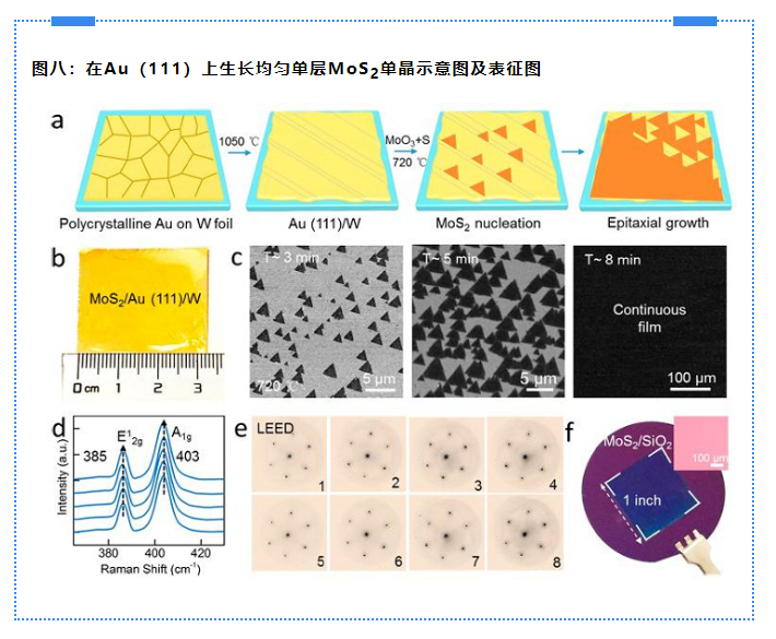
8. ACS Nano epitaxially grows centimeter-level single crystal MoS2 film on Au(111)
9. Advanced Materials two-dimensional ferromagnetic Cr2S3 semiconductor controlled growth and thickness conductivity dependence
Two-dimensional magnetic materials have attracted widespread attention as an ideal platform for constructing multifunctional electronic and spintronic devices. However, most of the reported two-dimensional magnetic materials are mainly realized by mechanical peeling, especially the thickness control synthesis up to the 2D limit. Peking University Zhang Yanfeng‘s research group used chemical vapor deposition and precisely controlled the feed rate and growth temperature of the Cr precursor to synthesize the thickness of nano-sized diamond-shaped Cr2S3 thin slices (about 1.9 nm to tens of nanometers) on a chemically inert mica substrate. With the increase of the thickness of Cr2S3 nanosheets (from 2.6 nm to 4.8 nm, >7nm), the conduction behavior of Cr2S3 changes from p-type to bipolar type to n-type. This work provides new insights for elucidating the scalable synthesis, transmission and magnetic properties of 2D magnetic materials. [9] Related results were published on Adv. Matter. with the title "Controlled Growth and Thickness-Dependent Conduction-Type Transition of 2D Ferrimagnetic Cr2S3 Semiconductors".
10. Nanoscale nickel sulfide modification improves the electrocatalytic activity of amorphous molybdenum sulfide nanosheets
Amorphous nano-sized MoSx (a-MoSx) has abundant active sites and expandable synthesis capabilities, and is an attractive electrocatalyst for hydrogen release reaction (HER). However, it is still a challenge to clarify the internal catalytic mechanism and achieve higher HER performance in a scalable size. The research group of Wang Xina of Hubei University and the research group of Zhang Yanfeng of Peking University successfully synthesized a-MoSx flakes decorated with Ni3S2 nanocrystals (size <10 nm) on a Ni foam of 10×20 cm2 by portable hydrothermal method. catalyst. The combination state and Raman characterization proved the strong interaction between [Mo3S13]2-cluster and Ni3S2; the perfect interfacial polymerization between [Mo3S13]2-cluster itself and [Mo3S13]2-cluster and Ni3S2 through density functional theory The calculation is confirmed. These two factors greatly reduce the absorption energy of hydrogen to almost zero, thereby greatly improving HER activity. The current densities of 100 and 600 mA cm-2 were achieved at overpotentials of 181 and 246 mV, respectively. This work provides a basic reference for the catalytic origin of a-MoSx-based catalysts, and provides practical applications for the compatibility of non-noble metal electrocatalysts with low-cost mass production. [10] Related results were published in Nanoscale with the title "Boosting the electrocatalytic activity of amorphous molybdenum sulfide nanoflakes via nickel sulfide decoration".
references:
This information is from the Internet for academic exchanges. If there is any infringement, please contact us and delete it immediately
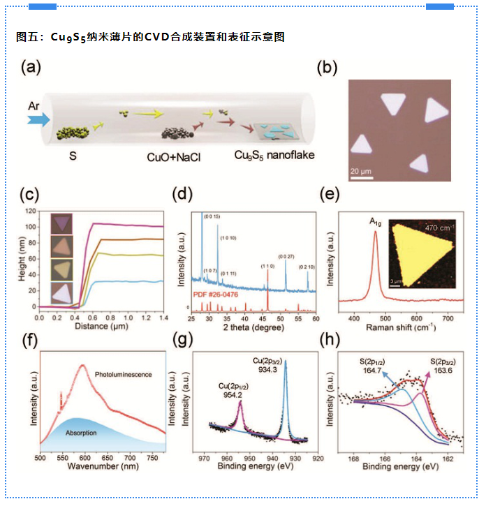

Figure 7: Schematic diagram and characterization diagram of O2 plasma treatment technology
Zhang Yanfeng (Peking University)
Two-dimensional (2D) semiconductor transition metal sulfide (TMD) has become an attractive platform for the next generation of nanoelectronics and optoelectronics. The controlled synthesis of wafer-level single-crystal TMD with high crystallinity has always been an unremitting pursuit. However, epitaxial growth of TMD films on insulating substrates (such as mica and sapphire) fails to eliminate the development of antiparallel domains and twin boundaries, resulting in the formation of polycrystalline films. Peking University Zhang Yanfeng’s research team and Tsinghua University and others have reported that polycrystalline Au foil is converted into centimeter-level Au(111) film through the melting-solidification method, and this is used as a substrate for van der Waals epitaxy to realize a single-layer MoS2 nanosheet The single-oriented growth of centimeter level (1 inch) single crystal monolayer MoS2 film was obtained. Through the combination of scanning tunneling microscope characterization and first-principles calculations, it is found that the nucleation of MoS2 monolayer is mainly guided by the upper step of Au (111), which leads to the directional growth of MoS2 along the height of the step edge of ⟨110⟩. This research has developed a new method/new system for preparing large-area single-layer MoS2 single-crystal thin film by epitaxy on a metal single-crystal substrate, and in-depth analysis of its growth mechanism, which provides a possibility for wafer-level preparation of high-quality two-dimensional materials The solutions and research ideas are of great significance to the promotion of device integration and practical application of semiconductor two-dimensional materials. [8] Related results were published in ACS Nano with the title "Epitaxial Growth of Centimeter-Scale Single-Crystal MoS2 Monolayer on Au(111)".


1. Wang Y., Wang S., Zhang S., Lou X., Formation of Hierarchical FeCoS2-CoS2Double-Shelled Nanotubeswith Enhanced Performance for Photocatalytic Reduction of CO2, [J] Angew. Chem. Int. Ed. 2020, 59, 1-6.
2. Fang Y., Luan D., Chen Y., Gao S., Lou X., Rationally Designed Three-Layered Cu2S@Carbon@MoS2Hierarchical Nanoboxes for Efficient Sodium Storage, [J] Angew. Chem. Int. Ed. 2020 , 59, 7178-7183.

| Reminder: Beijing Beike New Material Technology Co., Ltd. supplies products only for scientific research, not for humans |
| All rights reserved © 2019 beijing beike new material Technology Co., Ltd 京ICP备16054715-2号 |
