Two-dimensional materials refer to materials in which electrons can only move freely (planar motion) on non-nanoscale (1-100nm) in two dimensions, such as nano-films, superlattices, and quantum wells. Currently, two-dimensional materials have become countries Research focus. Beike Nano can provide customers with two-dimensional material research program design, device fabrication and device performance testing such as field effect tubes, Hall bar), Beike Nano can provide customers with two-dimensional material device design, production and performance testing services , And also provide customers with the preparation of high-performance two-dimensional materials such as graphene, molybdenum disulfide, tungsten disulfide, black phosphorus, etc.
Two-dimensional materials have rich physical properties and diversified device applications, and can be widely used in various fields such as photodetectors, optoelectronic devices, memories, logic operation elements, light-emitting diodes, and lasers. Provide customers with design, manufacturing and testing services of two-dimensional material devices.
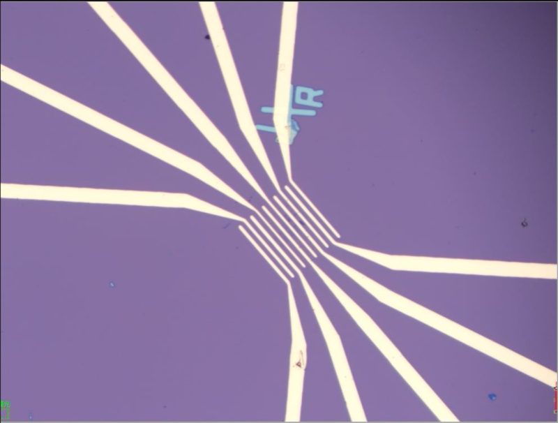
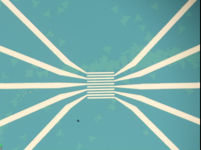
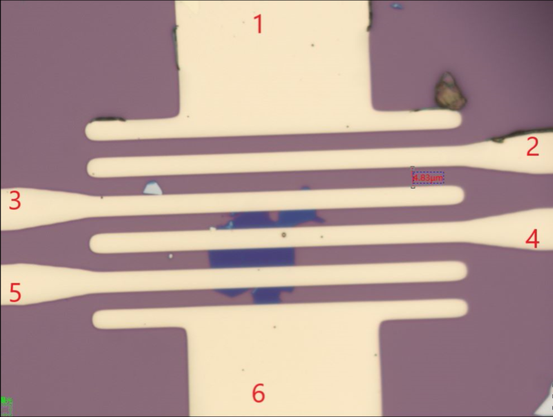
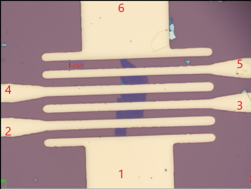
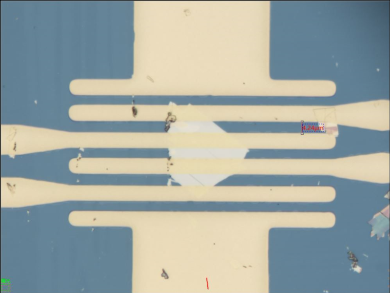
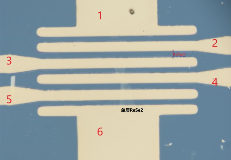
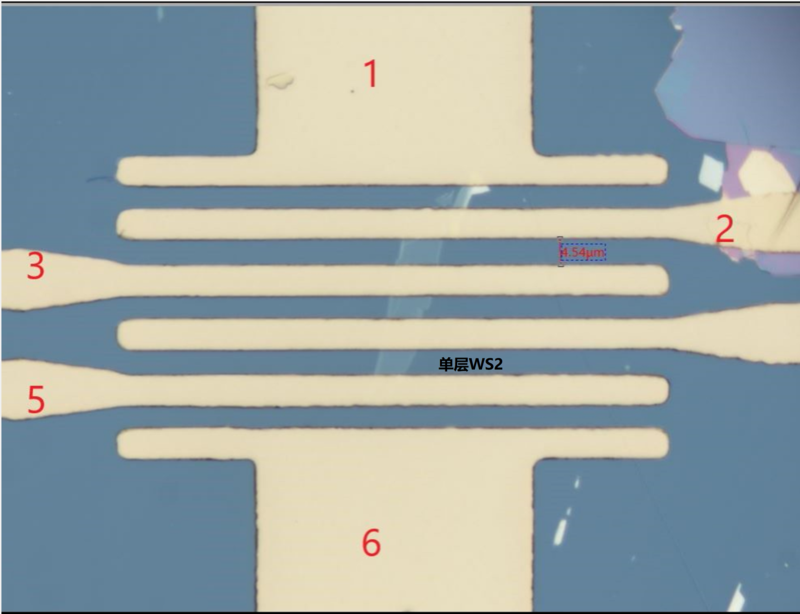
Field effect tube, Hall Bar
(The structure diagram of the field effect tube under the optical microscope)
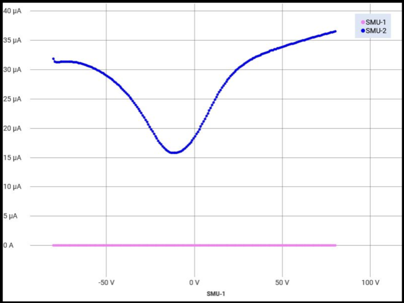
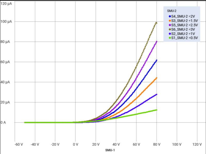
(FET test output and transfer curve)
Preparation of two-dimensional materials
Two-dimensional materials, as the characteristics of unit elements in electrical and optoelectronic systems, have the ability to integrate with complementary metal oxide semiconductor technology and have been widely studied in various fields. To help scientific research, Beike Nano can provide customers with the preparation of the following two-dimensional materials.
|
BP series
|
BP series
|
|
BP block (high quality,> 500mg)
|
|
b-AsxP1-x (0.2 ‘<‘ x <0.9) black arsenic phosphorus alloy
|
|
Se-doped BP
|
|
Te-doped BP Tellurium-doped BP
|
|
MPX3 series
|
FePS3 iron phosphorus sulfur
|
|
FePSe3 iron phosphorus selenium
|
|
NiPS3 nickel phosphorus sulfur
|
|
NiPSe3 nickel phosphorus selenium
|
|
MnPS3 manganese phosphorus sulfur
|
|
MnPSe3 Manganese Phosphorus Selenium
|
|
CrPS4 Chromium Phosphorus Sulphur
|
|
TIs are absolutely topological
|
Bi2Se3 Bismuth Selenide
|
|
Bi2Te3 Bismuth Telluride
|
|
Sb2Te3 Antimony Telluride
|
|
Ternary narrow band gap
|
Ta2NiS5
|
|
Ta2NiSe5
|
|
Ga series
|
GaS gallium sulfide
|
|
GaSe Gallium Selenide
|
|
V Series TMDs
|
1T-VS2 vanadium disulfide
|
|
1T-VSe2 Vanadium diselenide
|
|
1T-VTe2 Vanadium Telluride
|
|
Ti series TMDs
|
1T-TiS2 titanium disulfide
|
|
1T-TiSe2 titanium diselenide
|
|
1T-TiSxSe2-x
|
|
Sn-based TMDs
|
2H-SnS2 tin disulfide
|
|
2H-SnSe2 tin diselenide
|
|
2H-SnSxSe2-x
|
|
Ta series TMDs
|
1T-TaS2 tantalum disulfide
|
|
2H-TaSe2 tantalum diselenide
|
|
2H-TaSxSe2-x
|
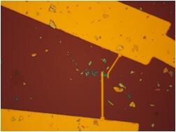
(Black phosphorus)
|
Warm tip: the products supplied by Beijing Beike Xincai Technology Co., Ltd. are only used for scientific research, not for human body |