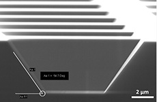
Etch (Etch) is a technique for selectively etching the surface of a semiconductor substrate or a surface covering film according to mask patterns or design requirements. It is one of semiconductor manufacturing processes, microelectronic IC manufacturing processes, and micro-nano manufacturing processes Quite an important step. It is a main process of pattern processing related to photolithography. Etching is divided into dry etching and wet etching. Beike Nano currently masters various etching processes, and will design etching solutions with good etching effect and high cost performance according to customer needs.
Technology application
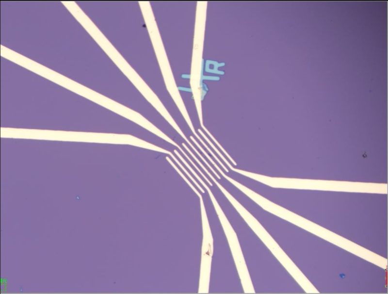
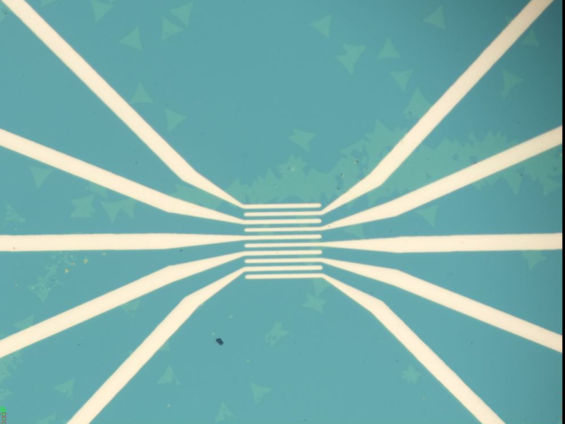
Etching technology is mainly used in the processing of semiconductor devices, integrated circuit manufacturing, thin film circuits, printed circuits and other fine patterns.
Process capability
Etching technology:
Etching techniques such as ion beam etching, deep silicon etching, reactive ion etching, and focused ion beam
Etching materials ::
Silicon, silicon oxide, silicon nitride, metal, quartz and other materials
Our advantage
Master multiple etching techniques Wide range of etching materials Deep silicon etching maximum aspect ratio 20: 1 High etching precision and small line width
|
Warm tip: the products supplied by Beijing Beike Xincai Technology Co., Ltd. are only used for scientific research, not for human body |