Bonding is a technology that directly cleans and activates two pieces of homogenous or heterogeneous semiconductor materials with clean surface and atomic level smoothness under certain conditions, and combines wafer bonding into a whole through van der Waals force, molecular force and even atomic force. Bonding is one of the important steps in the MEMS process. Choosing the best bonding process can ensure the mechanical stability, sealing and device satisfaction of the device. We currently have a variety of bonding technologies and mature processes to meet various customer requirements for different substrates, thicknesses, temperatures, and pressures.
Technology application
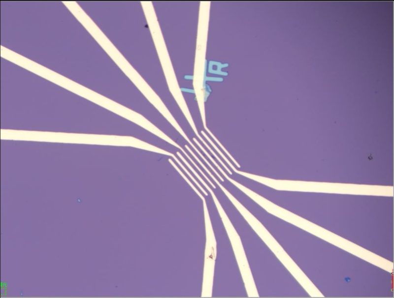
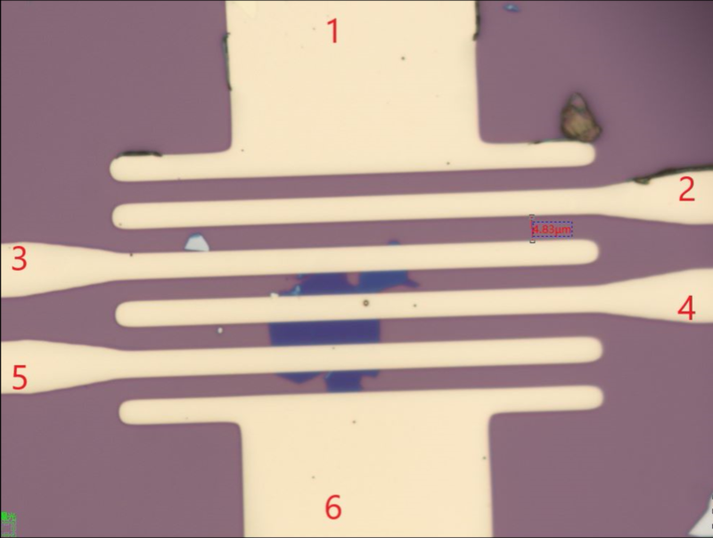
Bonding technology is widely used in the production process of microelectronic devices, such as microcavity devices, cantilever beam devices, sacrificial layers, and the production of special structures.
Process capability
Anodic bonding Eutectic bonding (AuSn, CuSn, AuSi, etc.) Adhesive bonding (AZ4620, SU8, bonding special adhesive)) Wire bonding
Our advantage
In a 100-level clean environment Rich bonding process High bonding strength
|
Warm tip: the products supplied by Beijing Beike Xincai Technology Co., Ltd. are only used for scientific research, not for human body |