- Home
- About Us
- Custom
- Product
- nano frontiers
- Hydrogels
- Quantum dots
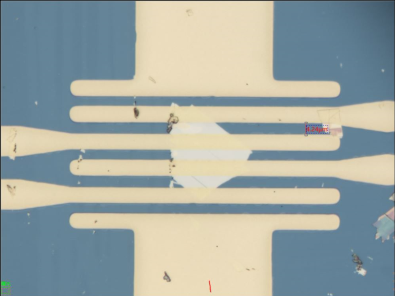
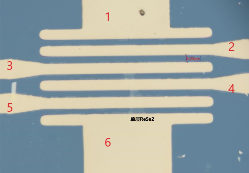
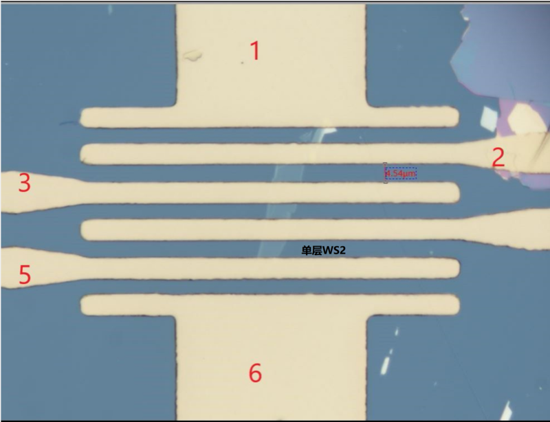
- Micro-nano processing
- Nanozyme
- COFs
- Summary
- Sulfide
- MOFs
- Battery energy storage
- Graphene Biomedicine
- Mxene Biomedicine
- MOFs Biomedicine
- Quantum dots phosphorus Biomedicine
- Black phosphorus Biomedicine
- Metal Biomedicine
- COFs Biomedicine
- 2D TMDC Dynamics
- Daniel Dynamic Frontier
- Perovskite dynamics
- Bio-nanomedicine
- Graphene carbon nanotubes
- Nanocellulose
-
Material calculation
- Nanomedicine - Cosmetic Surgery
- Nanomedicine - Burn Department
- Nanomedicine ― Urology
- Nanomedicine―Orthopedics
- Nanomedicine―Hepatobiliary and Pancreatic Surgery
- Nanomedicine - Vascular Surgery
- Nanomedicine ― Gastrointestinal Surgery
- Nanomedicine―Head and Neck Surgery
- Nanomedicine - Hematology
- Nanomedicine - Rheumatology and Immunology
- Nanomedicine - Neurology
- Nanomedicine―Respiratory
- Nanomedicine―Digestive
- Nanomedicine - General Internal Medicine
- Nanomedicine - Endocrinology
- Nanomedicine - Tumors
- Nanomedicine - Cardiovascular
- Beike Material Computing Service
- Frontiers of Material Computing
- Material customization
- MXene frontiers
- Contact Us
- 中 文