

 Beike Laboratory
Device Microfabrication R&D Laboratory
QQ Academic Group: 1092348845
Detailed
Beike Nano Devices has independently built a complete micro-nano device test line. The main equipment includes:
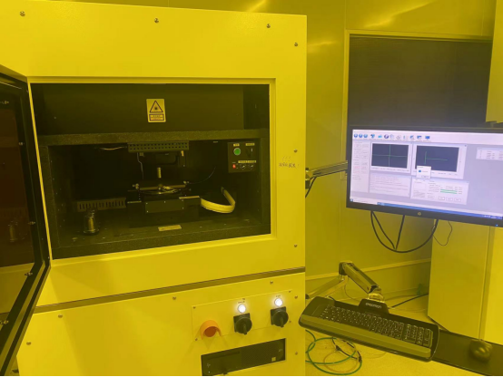
Laser direct writing exposure machine:
Exposure wavelength 405nm
Direct writing area: maximum 100*100mm
Exposure accuracy: minimum 2um
It is suitable for arbitrary graphic writing, and does not require a mask when writing patterns directly. It can also be used to make masks for contact lithography machines.
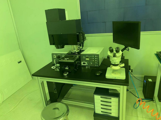
Contact UV Exposure Machine
Exposure wavelength 365nm
Exposure area, 4 inches
Exposure accuracy 1um
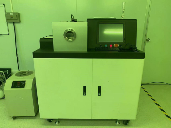
RIE reactive ion etching machine
Process gas: CF4, SF6, O2, Ar
For the etching of two-dimensional semiconductor films, graphene and other thin-film materials. It can also be used for the etching of semiconductor materials such as silicon, silicon oxide, and glass.
The etching depth is generally not more than 2um.
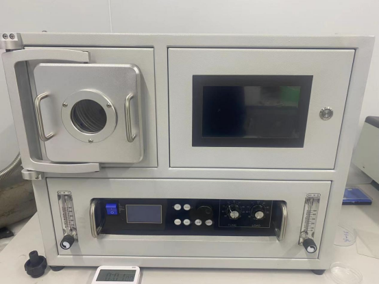
Plasma cleaner
Process gas: Ar, O2
For graphene etching, plasma degumming and other processes.
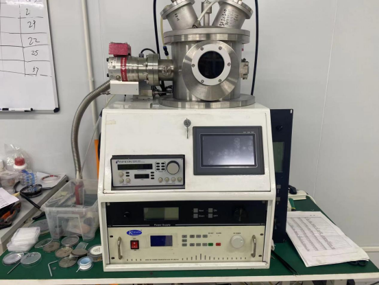
Thin film deposition:
Electron beam evaporation coating machine No. 1 (for metal coating).
Dedicated to the deposition of commonly used metal electrode materials such as gold, titanium, chromium, bismuth, antimony, silver, platinum, and palladium.
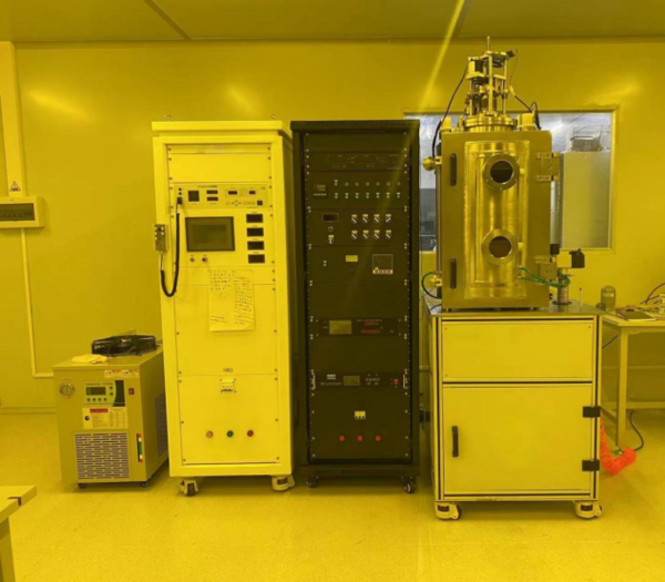
Electron beam evaporation coating machine No. 2 (special for dielectric film coating)
It is specially used for the deposition of dielectric film materials such as aluminum oxide Al2O3, silicon oxide, titanium oxide, vanadium oxide, titanium nitride, and silicon nitride.
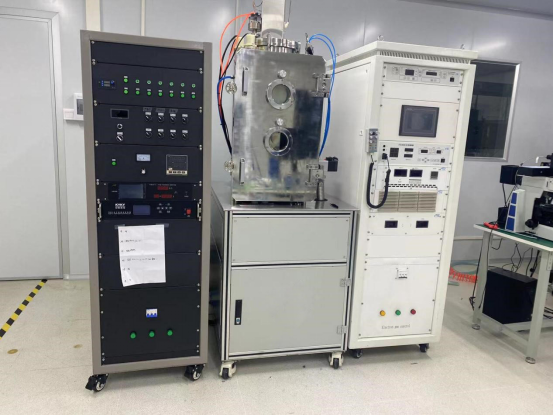
3 target magnetron sputtering coater (special for metal coating).
Specially used for metal DC magnetron sputtering coating and reflection sputtering coating.
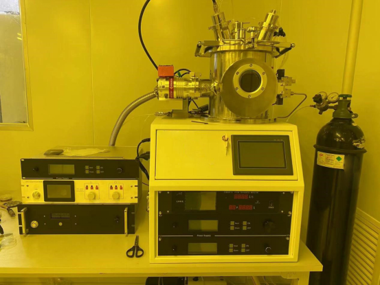
2 target magnetron sputtering coater (for dielectric film coating)
For metal DC magnetron sputter coating and RF sputter coating (non-conductive materials).
Auxiliary equipment:
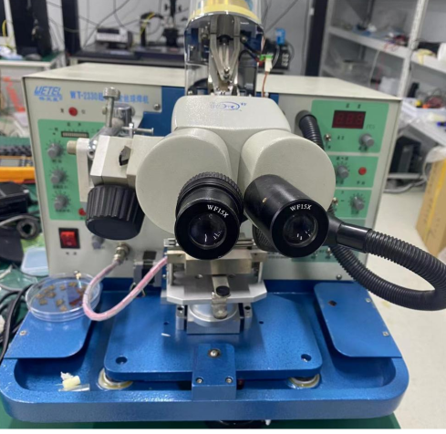
Gold wire binding bonding equipment
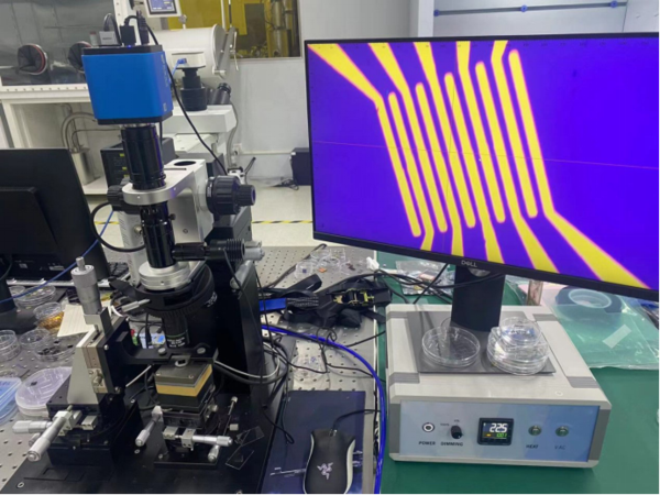
Two-dimensional material positioning and transfer equipment (heterojunction construction, positioning and transfer)
For 2D material localization transfer and heterojunction construction.
Other auxiliary equipment such as: various specifications of glue dispenser, incident etching table, pure water machine and other micro-processing supporting equipment.
For each device process step, the device laboratory has two sets of equipment based on different methods, which are backups for each other, which can ensure that the research and development process will not be interrupted due to equipment downtime, and speed up the time process of device demo.
In addition, based on research and development needs, Beike Nano is constantly researching or purchasing a variety of research and development equipment for special device processes, and promotes the research and development of devices based on cutting-edge materials to become practical as soon as possible.
Laser direct writing exposure machine:
Exposure wavelength 405nm
Direct writing area: maximum 100*100mm
Exposure accuracy: minimum 2um
It is suitable for arbitrary graphic writing, and does not require a mask when writing patterns directly. It can also be used to make masks for contact lithography machines.
Contact UV Exposure Machine
Exposure wavelength 365nm
Exposure area, 4 inches
Exposure accuracy 1um
RIE reactive ion etching machine
Process gas: CF4, SF6, O2, Ar
For the etching of two-dimensional semiconductor films, graphene and other thin-film materials. It can also be used for the etching of semiconductor materials such as silicon, silicon oxide, and glass.
The etching depth is generally not more than 2um.
Plasma cleaner
Process gas: Ar, O2
For graphene etching, plasma degumming and other processes.
Thin film deposition:
Electron beam evaporation coating machine No. 1 (for metal coating).
Dedicated to the deposition of commonly used metal electrode materials such as gold, titanium, chromium, bismuth, antimony, silver, platinum, and palladium.
Electron beam evaporation coating machine No. 2 (special for dielectric film coating)
It is specially used for the deposition of dielectric film materials such as aluminum oxide Al2O3, silicon oxide, titanium oxide, vanadium oxide, titanium nitride, and silicon nitride.
3 target magnetron sputtering coater (special for metal coating).
Specially used for metal DC magnetron sputtering coating and reflection sputtering coating.
2 target magnetron sputtering coater (for dielectric film coating)
For metal DC magnetron sputter coating and RF sputter coating (non-conductive materials).
Auxiliary equipment:
Gold wire binding bonding equipment
Two-dimensional material positioning and transfer equipment (heterojunction construction, positioning and transfer)
For 2D material localization transfer and heterojunction construction.
Other auxiliary equipment such as: various specifications of glue dispenser, incident etching table, pure water machine and other micro-processing supporting equipment.
For each device process step, the device laboratory has two sets of equipment based on different methods, which are backups for each other, which can ensure that the research and development process will not be interrupted due to equipment downtime, and speed up the time process of device demo.
In addition, based on research and development needs, Beike Nano is constantly researching or purchasing a variety of research and development equipment for special device processes, and promotes the research and development of devices based on cutting-edge materials to become practical as soon as possible.
- Previous: Materials R&D Laborato
- Next: Materials Characteriza