
1. Article overview
Although Ti3C2Tx MXene nanosheets have high conductivity, it is still a challenge to design highly stretchable MXene electrodes for use in flexible electronic devices. Inspired by the high extensibility of paper-cut patterns, the research team of teachers Hao-Bin Zhang and Zhong-Zhen Yu of Beijing University of Chemical Technology recently reported a bottom-up method, by constructing a wrinkled MXene pattern on a flexible PDMS substrate. Create a layered surface with primary and secondary surface wrinkles. Highly stretchable, conductive polydimethylsiloxane (PDMS)/Ti3C2Tx MXene film can be designed for electromagnetic interference (EMI) shielding and pressure sensing application. Related research work titled "Kirigami-Inspired Highly Stretchable, Conductive, and Hierarchical Ti3C2Tx MXene Films for Efficient Electromagnetic Interference Shielding and Pressure Sensing" was published in the top international journal ACS Nano (IF=14.588), which attracted widespread attention in this field .
Two, graphic guide
(1) During the pre-stretching/release cycle, the self-controlled microcracks generated by uneven deformation in the valley region of the layered film endow the layered PDMS/MXene film with high stretchability (100%). It has stable electrical conductivity in the range of %-100% strain and stable electrical conductivity in 1000 cycles of fatigue measurement.
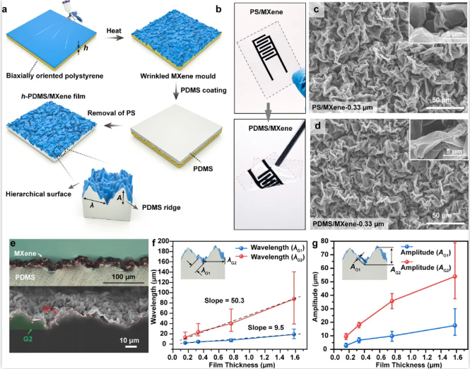
Figure 1. (a) Schematic diagram of the production of a layered PDMS/MXene film with wrinkled MXene layer.
(B) Photographs of wrinkled PS/MXene and PDMS/MXene films.
(C) SEM images of wrinkled PS/MXene film and (d) wrinkled PDMS/MXene film.
(E) Cross-sectional optical image (top) and SEM (bottom image) of the wrinkled PDMS/MXene film.
(F) The correlation between the wrinkle wavelength and (g) the amplitude of the PDMS/MXene film on the thickness of the MXene layer.
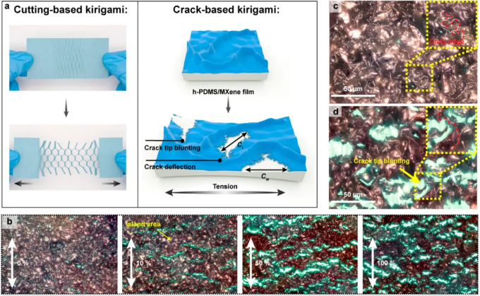
Figure 2. (a) Schematic diagram of the crack evolution of cut-based paper-cut film, crack-based paper-cut film and h-PDMS/MXene film during stretching.
(B) The surface morphology evolution of h-PDMS/MXene film during stretching.
The ridge structure (c) does not have and (d) has 100% tensile strain.
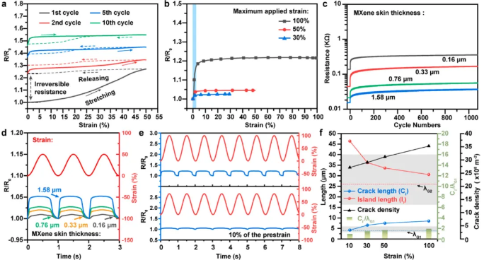
Figure 3. (a) The relationship between the resistance change of the h-PDMS/MXene film and the applied strain.
(B) The relationship between the resistance change of the h-PDMS/MXene film and the maximum applied strain.
(C) Cycle test of h-PDMS/MXene membrane.
(D) Strain time (ST) and resistance time (RT) curves of h-PDMS/MXene film.
(E) S-T and R-T curves of h-PDMS/MXene film without (top) and with a prestress of 10% (bottom).
(F) Graphs of crack length, island length and crack density of h-PDMS/MXene film under different strains.
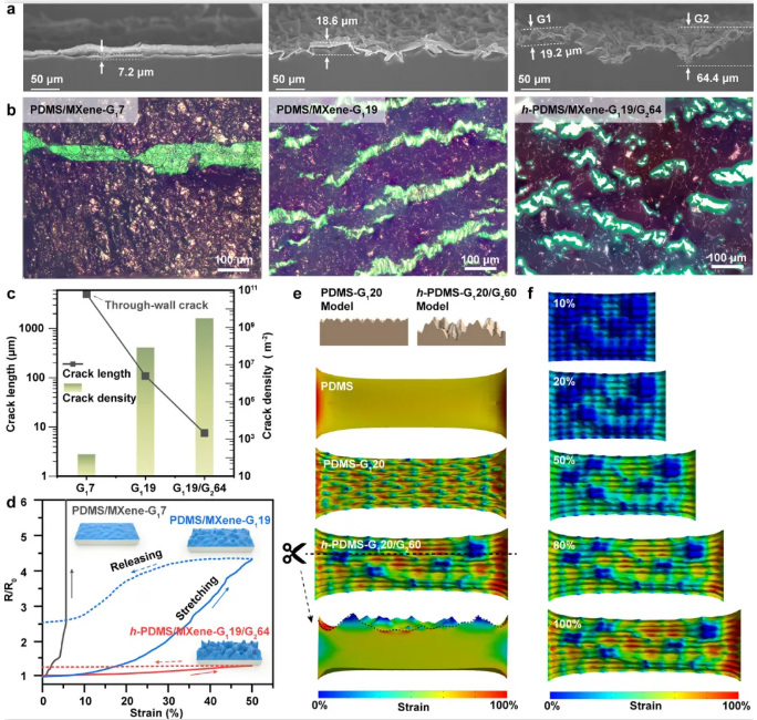
Figure 4. (a) Cross-sectional SEM images of layered PDMS/MXene films with different ridge heights.
(B) Surface morphology and (c) crack density and length of layered PDMS/MXene films with different ridge heights at a tensile strain of 50%.
(D) The resistance change of PDMS/MXene layered films with different ridge heights under 50% tensile strain.
(E) Through finite element analysis, strain distribution of PDMS, PDMS-G120 and h-PDMS-G120/G260 films.
(F) Through finite element analysis, the strain distribution of h-PDMS-G120/G260 film under different strains.
(2) The stretchable film exhibits a highly stable EMI shielding performance of about 30 dB under a tensile strain of 50%, and by constructing a two-layer film structure, its EMI shielding efficiency is further improved to 103 dB.
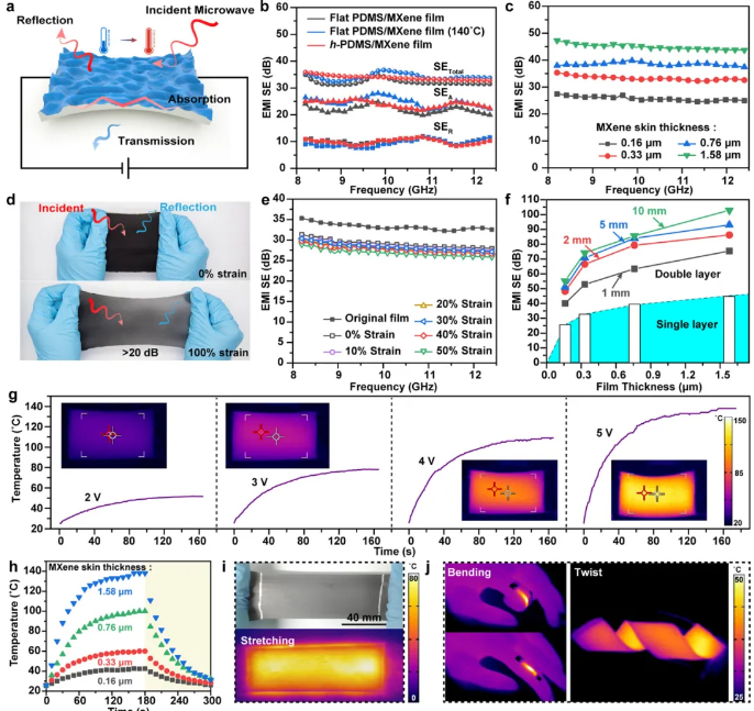
Figure 5. (a) Schematic diagram of EMI shielding and Joule heating of h-PDMS/MXene film.
(B) h-PDMS/MXene film, flat PDMS/MXene film and flat PDMS/MXene film are annealed at 140°C and have the same EMI shielding performance of MXene layer thickness.
(C) EMISE diagrams of h-PDMS/MXene films with different MXene layer thicknesses.
(D) Optical photograph of h-PDMS/MXene film used for EMI shielding under tensile deformation.
(E) The relationship between EMISE of h-PDMS/MXene film and applied strain.
(F) The relationship between EMISE and MXene skin thickness of single-layer and double-layer h-PDMS/MXene films.
The Joule heating performance of h-PDMS/MXene film (g) at different voltages and (h) at different MXene thicknesses.
(I) Infrared camera image and photograph of h-PDMS/MXene film under tensile strain.
(J) Thermal imaging camera image of h-PDMS/MXene film under twisting and bending.
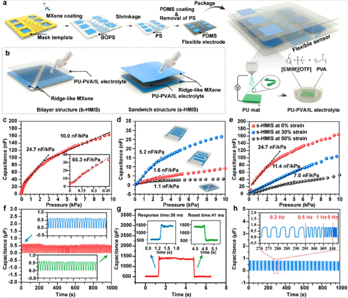
Figure 6. (a) illustrates the preparation process of the PDMS/MXene-based touch sensor.
(B) The layered structure of the touch sensor.
(C) Pressure-capacitance response of s-HMIS.
(D) Pressure-capacitance response of b-HMIS with different number of electrode pairs.
(E) The pressure-capacitance response of s-HMIS under different tensile strains.
(F) Durability test of s-HMIS under 90° bending angle.
(G) Response time and reset time of s-HMIS.
(H) Frequency response performance of s-HMIS.
(3) In addition, highly integrated MXene-based electrodes and circuits are manufactured through a stencil printing process, which can be used for highly stretchable and sensitive ionizing sensor arrays with high sensitivity (66.3 nF/kPa), It has excellent dynamic cycle stability in 1000 cycles at different frequencies, and has sensitive pressure monitoring capability under 50% tensile strain.
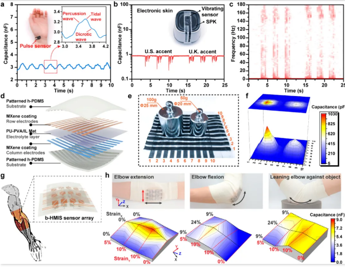
Figure 7. (a) The application of b-HMIS in pulse monitoring.
(B) The application of s-HMIS in detecting sound vibration, and (c) Short-term FFT (STFT) of the capacitance change signal.
(d) Schematic and (e) photograph of the s-HMIS sensor array, and (f) the corresponding capacitance distribution map.
(G) Schematic diagram of b-HMIS sensor array as a tactile sensor.
(H) Photograph of elbow joint movement and corresponding capacitance distribution map.
3. Thesis information
Kirigami-Inspired Highly Stretchable, Conductive, and Hierarchical Ti3C2Tx MXene Films for Efficient Electromagnetic Interference Shielding and Pressure Sensing
ACS Nano (IF=14.588)
Pub Date: 2021-04-16
https://doi.org/10.1021/acsnano.1c01277
Wei Chen, Liu-Xin Liu, Hao-Bin Zhang*, and Zhong-Zhen Yu*
Beijing Key Laboratory of Advanced Functional Polymer Composites, Beijing University of Chemical Technology, Beijing 100029, China


