
Research Background
Terahertz waves have a wide range of applications in medicine, communications, security, imaging, and non-intrusive quality testing. However, because of the low energy of terahertz photons, they are susceptible to thermal noise, and because of the lack of fast and sensitive THz photoelectric detector As well as high-performance portable THz sources operating at room temperature, the development of terahertz technology has been severely hindered. Two-dimensional materials have unique electronic and optoelectronic properties (such as ultra-fast charge transport and adjustable photon absorption, etc.), providing a broad platform for studying the quantum state of matter. The emergence of new two-dimensional material systems represented by graphene, transition metal chalcogenides, black phosphorus, and topological insulators has provided a new platform for terahertz detection. Recent studies have shown that two-dimensional materials have significant photo-thermoelectric effects (PTE). Non-equilibrium hot carriers are generated by absorbing terahertz to form a temperature gradient distribution. The use of field-effect regulation can achieve rapid extraction and signal modulation of non-equilibrium carriers. It can avoid the quantum limit problem of traditional single particle excitation and has the advantages of wide bandwidth and integration, so it is expected to achieve effective detection of terahertz at room temperature. The main obstacle to terahertz detection using the PTE effect at present is the huge mismatch between the incident wavelength and the relatively small photosensitive area, and the material‘s ability to absorb is weak, resulting in low responsiveness.
Similar to graphene, if there is asymmetry (such as asymmetric doping or antenna feedback), the photothermoelectric effect in black phosphorus (BP) is also the photothermally driven photoresponse through the interband process at THz frequency. Due to its in-plane anisotropy, BP exhibits high electrical and thermal conductivity. However, the photo-thermoelectric effect of BP has not been fully utilized in the infrared and THz bands.
Achievements
In view of this, recently, researcher Chen Xiaoshuang of Shanghai Institute of Technology, Chinese Academy of Sciences, associate researcher Wang Lin, and researcher Zhang Kai (co-corresponding author) of Suzhou Institute of Nanotechnology reported the sensitivity of photothermoelectricity (PET) based on ultrashort channel black phosphorus devices. Hertz detection and imaging. It is found through simulation that the ultra-short channel structure can effectively achieve terahertz electric field focusing and enhancement. When the channel size is much smaller than the terahertz wavelength and even exceeds the skin depth of the metal antenna, the terahertz electric field enhancement can reach 2 to 3 orders of magnitude. Greatly increase the probability of interaction between electrons and photons. Using BP as a channel material has the advantages of high carrier mobility, adjustable band gap with thickness, electrical conductivity, and thermally conductive in-plane anisotropy, which can promote the rapid transfer of hot electrons and photon absorption. The terahertz detector coupled with an ultra-short-channel (20 ~ 100 nm) asymmetric butterfly antenna was obtained by using an unconventional process and using a dip-second over-engraving technique to control different BP channel length structures. Excellent sensitivity of 297 V W-1, room-temperature noise equivalent power is less than 58 pW / Hz0.5, and response time is less than 0.8 μs, which is better than other room-temperature thermal-based detectors. Comparison with existing terahertz detectors, coupled with further optical pumping and imaging experimental verification, confirms the importance of local field effects in the skin limit, providing a new way to develop highly sensitive terahertz detectors Ideas. The article was published in the famous journal Advanced Science under the title "Sensitive Terahertz Detection and Imaging Driven by the Photothermoelectric Effect in Ultrashort-Channel Black Phosphorus Devices".
Graphic guide

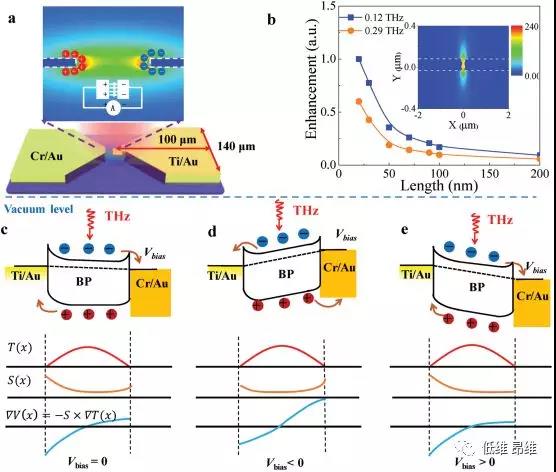
Figure 1. Ultra-short-channel PTE detector prepared by tilt technology. (A-d) Schematic diagram of device preparation process: (a, b) BP device with 4 μm long channel symmetrical electrode contact prepared in advance by UV lithography and stripping process. (C, d) Sub-100 nm channel and asymmetric electrode contact are formed in the BP photodetector after the inclination angle placement and stripping process after the second ultraviolet lithography. (E, f) Optical microscopy and AFM images of a BP sheet for device patterning. (G, h) Optical microscope and SEM images of a device with a 30 nm channel length and a magnified central region. (I, j) Raman spectrum and current-voltage characteristics of a 30 nm device. (K) The dependence of the channel length on the tilt angle θ.
In order to realize a terahertz detector with an ultra-short channel, as shown in FIG. 1, by using an inclination evaporation technique, an asymmetric electrode with a dissimilar metal can be realized. The multilayer BP was mechanically peeled onto a high-resistance Si substrate, and a 30 nm-thick slice was characterized by Raman and AFM (Figure 1f, i). Then, through UV lithography, electron beam deposition, and lift-off processes, the BP sheet was brought into contact with two butterfly antennas made of 10/60 nm (Cr / Au) metal stacks with a 4 μm gap (Figure 1b). In order to focus the incident THz radiation to a very small spot area, a second photolithography was performed specifically, a window was opened on the channel, and then electron beam deposition was performed along different tilt angles θ (Figure 1c). Hot carrier generation of photocurrent requires Seebeck coefficient gradient, so after the second photolithography, a 10/60 nm (Ti / Au) electrode was specifically deposited to form a sub-100 nm channel (Figure 1c). Finally, an ALD process was used to deposit 20 nm thick Al2O3 as a protective layer to avoid BP degradation (Figure 1d). By changing the evaporation angle θ, the length of the channel can be controllably reduced from 100 nm to 20 nm.

Figure 2. (a, b) Concept and simulation results of terahertz field enhancement: (a) Light-induced alternating current charges a sub-100 nm slit, resulting in local electric field enhancement, as shown by the gradient color outline. (B) The THz field distribution of the antenna cross section (white dashed line) and the sub-100 nanometer channel at 0.12 and 0.29 THz is enhanced by about two orders of magnitude at the hot spot. (Ce) Band diagram and electron temperature T (x), Seebeck coefficient S (x) and potential gradient ∇V (x) at the sub-100 nm channel junction region formed by two different metal contacts. The distribution of S × ∇T (x). Over the entire length of the device, the light response is proportional to the integral of ∇V (x).
When a terahertz wave is incident on the antenna vertically, an alternating current is induced on the surface, which causes charges to accumulate near the edge of the antenna. When the gap (or channel) in the center of the antenna continues to decrease towards sub-wavelengths and below, the charge density at the edges increases accordingly, resulting in a greatly enhanced electric field (Figure 2a). The existence of the ultra-short channel greatly changes the amplitude of the terahertz field, which causes a hot spot-like distribution at the channel (Figure 2b). When the channel length is 30 nm, the field enhancement at 0.29 THz exceeds two orders of magnitude, indicating that the electromagnetic compression ratio exceeds 104. Figure 2c-e shows the working principle of the device: the electrons / holes in the multilayer BP are heated by the incident field at the hot spot, and two metal contact electrodes are used as heat sinks, resulting in a temperature gradient ∇T (x) with the channel The position x changes. Due to the different metal-induced doping at the two metal-BP interfaces, the Seebeck coefficient is asymmetric over the entire channel, and the hot electron diffusion produces a potential gradient ∇V (x). The total signal is ∇V (x) on the channel. Because of the asymmetry, the integral is not zero. When Vbias = 0 V, due to the poor work function of the metal, the net photocurrent can flow from Cr / Au to Ti / Au, and the holes will be more depleted. However, when a negative bias is applied from Cr / Au to Ti / Au, the Seebeck coefficient difference will decrease or even change its sign, causing the photocurrent to change its direction.
 Figure 3. (a) Electrical structure of a PTE device. THz radiation is focused by an off-axis parabolic mirror, where Ti / Au is grounded. (B) The impulse current response at various excitation frequencies shows the broadband nature of the dominant mechanism of the PTE effect. (C) Polarization dependence of a 30 nm device at 0.29 THz. (D, e) Comparison of response time between 30 nm and 4 μm devices. (F) Bias-dependent response of ultra-short-channel PTE devices and 4 μm-channel devices at 0.12 THz. (G-i) Photocurrent, response rate, and NEP vs. bias at 0.12 and 0.29 THz, respectively.
Figure 3b shows the time-resolved optical response of different incident photon frequencies at zero bias. All pulse shapes are well preserved and have a good signal-to-noise ratio, which indicates that the device is suitable for multi-band detection. , In line with the theoretical prediction of the subwavelength butterfly structure. When the terahertz electric field is parallel to the channel, the responsivity is the smallest, and when the terahertz electric field is perpendicular to the channel, the signal is increased by 120 times by exciting the AC charge oscillation, which eventually results in a leaf-like polarization pattern (Figure 3c). The single-cycle time response is shown in Figure 3d. The rise time of the PTE detector at zero bias is 0.8 μs and the fall time is 1.5 μs, which confirms the real-time imaging capability, and the rise / fall of the 4 μm channel length device response The time is about 15 μs (Figure 3e). By applying a positive bias, holes flow more easily from the Cr / BP interface to the Ti / BP interface, which increases the photocurrent and increases the photocurrent of the short-channel device even more (Figure 3f). Changes in photocurrent, response rate, noise equivalent power (NEP), and bias at 0.12 and 0.29 THz are shown in Figures 3g-i, which are superior to other heat-based drive detectors in terms of sensitivity and speed. Table 1 summarizes the performance of devices with different channel lengths obtained at different inclination angles. It can be found that when the channel length is reduced to 30 nm, the performance is still improving.


Figure 4. Infrared pumping of sub-100 nm channel detector in zero bias mode and detection using BP‘s terahertz radiation. (A) 3D schematic diagram of an infrared-assisted terahertz photocurrent response device. (B) Variation of the device‘s terahertz photocurrent response with the power of the infrared light source. (C, d) The Fermi level shift caused by optical pumping excitation eliminates the difference in Seebeck coefficient between the two metal-BP interfaces, just like an optical switch.
Because BP is a narrow-bandgap semiconductor, its photon absorption shows a wavelength dependence up to the mid-infrared wavelength. Visible / infrared light pumping is expected to be a feasible tool for further processing of unbalanced carrier distribution caused by terahertz waves. As shown in Figure 4a, a continuous optical pumped laser at 825 nm is uniformly irradiated onto the detector to control the carrier dynamics in the THz field. As the laser intensity increases, the THz light response decreases (Figure 4b). This phenomenon can be attributed to the thermal effects of near-infrared radiation, which eliminates the asymmetric distribution of non-equilibrium carriers and causes photocurrent bleaching. At the same time, the expansion of the non-equilibrium carrier distribution and the upward shift of the quasi-Fermi level result in a small Seebeck coefficient difference, further reducing the optical signal (Figure 4c, d)

Figure 5. (a) Optical photograph of fresh leaves used in imaging. (B) The 0.29 THz nondestructive transmission image of fresh leaves clearly shows the veins. (C) Optical photo of the metal key. (D) The terahertz image of the key encapsulated in the envelope. The BP-based terahertz detector can detect objects invisible to the human eye. (E) Schematic diagram of the device used for terahertz detection and imaging of macroscopic objects.
The device is placed at the focal point of the THz beam shown in FIG. 5e for a THz imaging application study. The terahertz source is tuned to 0.29 THz and operates at a repetition rate of 1 kHz at room temperature. The photodetector runs at zero bias and 20 ms integration time, and can clearly see the veins of the leaves and the key enclosed in the envelope, indicating that the PTE detector can be used for large area imaging.
Summary and outlook
In this paper, ultra-short channels as low as 30 nm are obtained by oblique metal deposition, and the photothermoelectric effect is used to improve the performance of THz photodetectors within the skin depth limit. The device exhibits high response capability higher than 297 V W-1, noise equivalent power lower than 58 pW Hz0.5, and fast response capability at a wide photon frequency, which is superior to other thermal-based detectors operating at room temperature. Terahertz imaging experiments show that BP-based PTE photodetectors have practical applications in biomedical sensing, non-destructive evaluation and quality control. It is expected to further improve the sensitivity of the room temperature THz detector through antenna optimization and material selection.
Literature information
Sensitive Terahertz Detection and Imaging Driven by the Photothermoelectric Effect in Ultrashort-Channel Black Phosphorus Devices (Adv. Sci., 2020, DOI: 10.1002 / advs.201902699)
Literature link: https://onlinelibrary.wiley.com/doi/10.1002/advs.201902699


