
Research Background
The realization of p-n junctions (through p and n doping) is essential for the fabrication of two-dimensional semiconductor devices with advanced functions such as logic and memory. Electrostatic doping, chemical doping, ion implantation, charge transfer, and annealing control can be used to regulate the type of carriers in two-dimensional materials, but controllable doping still has challenges. Once a p-n junction is formed, it is difficult to change its electrical characteristics other than the electrostatic doping method. However, electrostatic doping requires a voltage to maintain the carrier type, and this process consumes energy.
A new alternative is the use of iron electrodes and the non-volatile nature of the electrostatic field at the interface. It has been previously reported that on a pre-polarized rigid substrate (such as LiNbO3 and BiFeO3), the carrier type is regulated in TMDs based on ferroelectric domains, but in the pn junction regulated by ferroelectric domains, it is observed that the substrate leakage Caused by poor rectification characteristics. Unlike traditional ferroelectric oxides that require high deposition temperatures, copolymers of polyvinylidene fluoride and trifluoroethylene (P (VDF-TrFE)) can form strong organic ferroelectric materials. These polymer-based ferroelectrics can The spin-coating method is used to prepare two-dimensional materials with good van der Waals interface bonding to reprogram the ferroelectric domain pattern, which provides a new strategy for the design of new, controllable and integrated CMOS devices.
Achievements
In view of this, recently, a researcher from the Shanghai Institute of Technical Physics of the Chinese Academy of Sciences, Wang Jianlu, and Professor Zhou Peng (co-corresponding author) of Fudan University have jointly reported that a programmable transition metal chalcogenide homojunction can be regulated by nonvolatile ferroelectric domains. Scanning probes are used to control the polarization direction of ferroelectric polymers deposited on two-dimensional TMDs. Carrier injection can be defined and p-type and n-type doped. The lateral pn, np, nn, and pp can be arbitrarily same. Formation and change of mass. The MoTe2 p-n homojunction device constructed in this way exhibits high current rectification ratio (103) and good photoelectric characteristics (response of 1.5 A W-1). At the same time, non-conventional non-volatile memory devices such as electrical write and optical read memory are also constructed, which are not restricted by physical source, drain or gate electrode. Quasi-non-volatile (QNV) memory has a refresh time of 100 s. And 10 ��s write / erase speed. The article was published in the authoritative journal Nature Electronics under the title of "Programmable transition metal dichalcogenide homojunctions controlled by nonvolatile ferroelectric domains".
Graphic guide
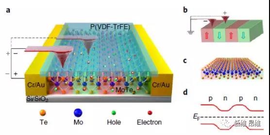
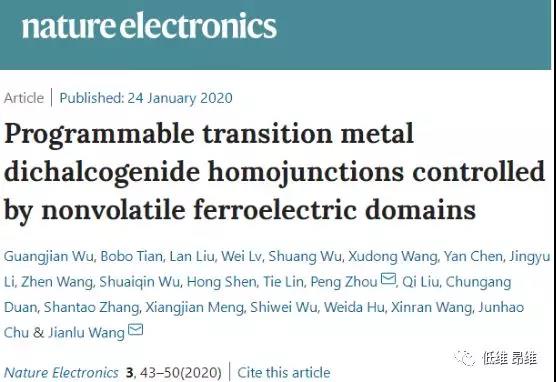
Figure 1. Spatially defined doping in MoTe2 using a ferroelectric field controlled by a piezoelectric response force microscope. (A) Schematic diagram of a periodic MoTe2 lateral p-n-p-n homojunction tuned using a probe-controlled ferroelectric domain. When the ferroelectric polymer is polarized downward (upward), electrons (holes) are injected into the channel. (B) The ferroelectric domain of P (VDF-TrFE) is locally controlled by the voltage applied to the probe. (C, d) The corresponding molecular configuration and band diagram of MoTe2.
Hexagonal phase (2H) MoTe2 was selected as a typical bipolar TMD. Figure 1a shows a schematic diagram of a two-dimensional MoTe2 covered by a ferroelectric P (VDF-TrFE) layer. The closed circuit of the conductive AFM probe is used as an electrode to polarize the ferroelectric copolymer covering MoTe2. The ferroelectric copolymers alternately polarized upward (Pup) and polarized downward (Pdown), so a lateral p-n-p-n junction structure was realized in MoTe2. The p-type doping comes from the accumulation (depletion) of holes (electrons) in MoTe2, which shields the polarized field in the Pup state. Conversely, n-type doping occurs in the Pdown state. Figure 1b shows a periodically polarized P (VDF-TrFE) film. The corresponding molecular configuration and band diagram of MoTe2 are shown in Figures 1c and d, respectively. With this method, carrier injection in TMD can be arbitrarily defined with nanometer-level accuracy. At the same time, iron electrodelation is switchable and non-volatile, so the carrier can be loaded without any physical constraints on the gate electrode. Stream type is regulated in situ.
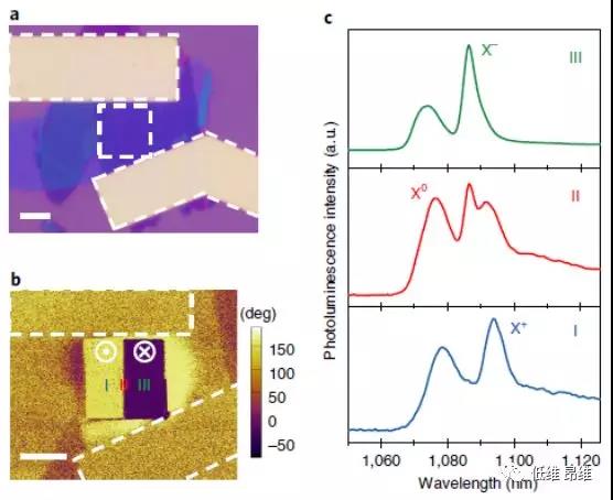
Figure 2. PL characteristics of a double-layer MoTe2 with ferroelectric field modulation at 6 K. (A) Optical micrograph of the device. A BN layer was inserted between MoTe2 and P (VDF-TrFE) to avoid luminescence quenching and the introduction of interface defect states at 6 K. White dotted lines mark the PFM working area and electrodes. (B) Corresponding PFM phase image. Regions I and III represent the Pup and Pdown states, respectively, and II represents the ferroelectric domain wall. The dots in the circle represent the Pup state, and the crosses in the circle represent the Pdown state. (C) PL spectra obtained from regions I, II and III.
The PL spectrum can be used to detect the type of doping in TMD. Figure 2a is an optical micrograph of the device. A BN layer is inserted between MoTe2 and P (VDF-TrFE) to avoid luminescence quenching and the introduction of interface defect states. This reduces the peak width and increases the intensity of the PL spectrum. First, when scanning the copolymer surface in AFM contact mode, the ferroelectric copolymer is polarized into two opposite polarization states by applying a bias voltage higher than the coercive voltage to the conductive probe. The PFM phase diagram is shown in Figure 2b Show. The regions with Pup and Pdown states are labeled I and III, respectively, and Region II represents 180 �� ferroelectric domain walls. PL spectra collected in three regions are shown in Figure 2c. In region I, the positively charged (X +) three sons (two holes and one electron) and the relatively weak neutral exciton (X0) dominate, which means that the holes in MoTe2 pass in the Pup state. Many, p-type doping occurs. In region III, the negatively charged (X-) three sons (two electrons and one hole) and X0 dominate, which indicates that the electrons in MoTe2 are excessive in the Pdown state, resulting in an intrinsic n-type doping. When the carrier type was adjusted from electrons to holes by the opposite polarization, the X0 peak was red-shifted at 4.7 nm, which was due to the band reformation caused by the increased doping. When the laser beam is irradiated on the region II, since the spot diameter (2 ��m) is larger than the size of the ferroelectric domain wall, an overlap of X +, X-, and X0 can be observed. These PL results indicate that the carrier type in MoTe2 can be changed by switching the iron polarization of the copolymer, and a p-n homojunction is formed at the position of the 180 �� domain wall.
Figure 3. MoTe2 p-n homojunction regulated by a ferroelectric field. (A) Top: Optical micrograph of the device. Middle: PFM phase diagram of P (VDF-TrFE). The area with a phase of -60 �� (dark) corresponds to the Pup state, and the area with a phase of 120 �� (yellow) corresponds to the Pdown state. MoTe2 is p-type in the Pup state and n-type in the Pdown state. Electrode 1 Connect 2, 2, and 3, 3 and 2, and 3 and 4 to pp, pn, np, and nn homojunctions. Bottom: Band structure of p-n junction. (B) Output curves (Isd-Vsd) of p-p, p-n, n-p and n-n homojunctions. (C) Isd-Vsd curves of p-n and n-p homojunctions plotted on a semi-logarithmic scale, suitable for Shockley diode models. (D) When Vsd = 1V, the Isd-Vg curves in different polarization states are compared with those before polarization (red curve), and the transition curves in Pup (gray curve) and Pdown (orange curve) are right / left. mobile. (E) Isd-Vsd curves (Vsd applied between electrodes 2 and 3) in the four-phase configuration of the ferroelectric copolymer (P1, P2, P3, and P4, respectively).
Rectification is a typical feature of a pn homojunction. Figure 3a shows an optical micrograph of a MoTe2 device used for electrical transport measurements. The PFM phase diagram shows that the ferroelectric copolymer is uniformly patterned into two domains with 180 �� The opposite ferroelectric domain of the wall, the band structure of the ferroelectrically induced pn junction is given at the bottom of Figure 3a. Figure 3b shows the output curves (Isd-Vsd) of these homojunctions, where the voltage is swept across the front electrode and the rear electrode is grounded. Compared with the non-polarized state, strong rectification behavior is observed in both the pn and np homojunctions, while the Isd-Vsd curves of the pp and nn homojunctions are almost symmetrical, and are significantly greater than those of the pn and np homojunctions at small bias Mass junction, which indicates that the strong rectification characteristics originate from the pn (np) homojunction, rather than the Schottky barrier between MoTe2 and the electrode. According to the fitting of the Shockley diode equation (Figure 3c), the ideal factors n of the diodes for p-n and n-p homojunctions are 2.5 and 2.5, respectively, indicating that the current is mainly determined by recombination rather than diffusion. Figure 3d shows the Isd-Vg curves for different polarization states when Vsd = 1 V. For the original state, the transfer curve exhibits typical bipolar characteristics, and the position of the minimum value is slightly greater than zero; for the Pup state, the minimum value of the transfer curve has shifted to the right by 40 V, and the upward polarization results in hole accumulation in MoTe2. A non-volatile shift occurs in the doped energy level, which moves the Fermi level toward the valence band; for the Pdown state, the minimum value of the transition curve has shifted to the left by 24 V. The PFM four-phase diagrams (P1, P2, P3, and P4) of the ferroelectric copolymer and the corresponding Isd-Vsd curves are shown in Figure 3e. The p�Cn homojunction and the corresponding rectification characteristics can be reversed, erased, and repeated. write.
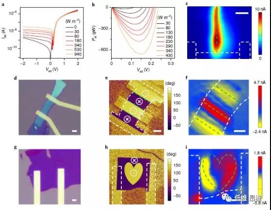
Figure 4. Optical response of p-n junctions and devices with other ferroelectric domain patterns. (A) Isd-Vsd curves of representative p-n homojunctions at 658 nm wavelength and different illumination powers from 0-940 W m-2. (B) The electric power extracted in a (Pel = Isd �� Vsd). (C) A spatial photocurrent map obtained by scanning a beam (wavelength 520 nm, power 1 ��W, spot size 2 ��m) on the sample with zero bias. The photocurrent appears exactly on the ferroelectric domain wall and is marked with a green dotted line. (Di) Write other ferroelectric domain patterns and corresponding PFM phase diagrams and space photocurrent diagrams on MoTe2 with different layers. The wavelength of the diode laser is 520 nm, and the power is 50 nW (f) and 500 nW (i). .
The optical and electrical properties of MoTe2 p-n homojunctions tuned by nonvolatile ferroelectric domains were subsequently investigated. Fig. 4a shows the Isd-Vsd curve of a representative p-n homojunction at a series of illumination powers P at a wavelength of 658 nm. Obvious photovoltaic effects are observed. As a photodetector, the p-n junction usually works at zero or reverse bias to achieve low dark current and high detection rate. When Vsd is 0, the response rate is 1.5 A W-1. Scan the light beam (wavelength 520 nm, power 1 ��W, spot size 2 ��m) on the sample with zero bias to obtain a spatial photocurrent map. The photocurrent appears exactly on the ferroelectric domain wall, and the contact between the electrode and MoTe2 is not Observation of the light response indicates that the potential barrier of the pn homojunction rather than the Schottky contact dominates the light response. Figure 4b shows the electric power when the laser power is 0-430 W m-2, and the power conversion efficiency �� is about 2.98%. The periodic pattern of pnpn MoTe2 is shown in Figure 4d�Cf. Four ferromagnetic domains with opposite polarization states between adjacent magnetic domains generate pn, np and pn homojunctions at three 180 �� magnetic domain walls. The corresponding space photocurrent diagrams of the three homojunctions are shown in Figure 4f. The photocurrents of opposite polarities indicate the existence of a reverse built-in electric field between the pn and np regions. A homojunction with an irregular shape (for example, a heart shape) once again proves that the ferroelectric domain pattern can be manipulated arbitrarily (Figure 4g-i).
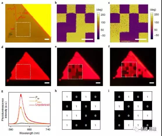
Figure 5. Electrical writing and optical reading memory arrays using arbitrary ferroelectric domain patterning. (A) Optical micrograph of single-layer WS2 device and AFM height profile. (B, c) PFM phase diagram of a 4 �� 4 ferroelectric domain pattern array obtained in a white area by a PFM probe. (D-f) The spatially resolved PL image of WS2 is highly consistent with the ferroelectric domain patterns written in b and c. (G) PL spectra taken from different polarization states. (H) Memory information image extracted from e. (I) Memory information image extracted from f.
WS2 shows extremely high PL intensity in the visible light band (~ 620 nm). When the WS2 is regulated by the Pup and Pdown states of the ferroelectric copolymer, different PL intensities are used to obtain "0" and "1" storage states, respectively. . Figure 5a shows an optical micrograph of a single-layer WS2 device. The ferroelectric domains are patterned in a white box. Figure 5d shows a spatially resolved PL image showing the homogeneity and strong PL characteristics of the sample. First, a 4 �� 4 ferroelectric domain pattern array is written using an AFM probe. As shown in the PFM phase diagram of FIG. 5b, a region with a phase of 180 �� corresponds to the Pup state, and a region with a phase of 0 �� corresponds to the Pdown state. The corresponding spatially resolved PL image is shown in Figure 5e. Each cell in the 4 �� 4 matrix shows a light or dark PL signal, which is consistent with the ferroelectric domain pattern in Figure 5b. The electrons are injected into WS2 in the Pdown state, resulting in a negatively charged triad. The reorganization is enhanced, so the PL intensity of the Pdown state is significantly stronger than that of the Pup state. A stored information image is created based on "0" and "1", as shown in Figure 5h. Reversing the ferroelectric domain of each cell, as shown in the PFM phase diagram of Figure 5c, the light and dark cells in the spatially resolved PL image are reversed (Figure 5f), providing the same results as in Figure 5h. Image complementary to the new memory information image (Figure 5i). This shows that the stored information related to polarization can be rewritten to achieve electrical writing and optical reading.

Figure 6. Electrical characteristics of p-n junction-assisted QNV memory. (A) Schematic of QNV memory. (B) Optical micrographs of typical devices. WSe2-1, WSe2-2, hBN, Gr-1, and Gr-2 represent the charge injection layer, channel, barrier layer, electrode contact layer, and charge trapping layer, respectively. (C) The PFM phase image of the highlighted area in the red dotted frame in b. Before and after polarization of (d, e) P (VDF-TrFE) film, stimulated by �� 4 V pulse on the FG electrode, Vsd = 1 V in-situ current. (F) Band diagrams of QNV memory used for write and erase processes, respectively. (G, h) After removing +4 V (g) and -4 V (h) pulse excitation on the FG electrode, Vsd = 1 V in-situ current, pulse width ranging from 10 ms to 10 ��s, "0" state It is a low-current state of 1 pA, indicated by a black dotted line. (I) The relationship between the current state and the width of the write / erase voltage pulse.
QNV memories can be constructed using ferroelectric domain patterns. In this structure, the graphene-2 (Gr-2) charge trapping layer in a floating gate (FG) memory is successfully connected to the outside via a WSe2 pn junction programmed with a ferroelectric domain pattern ( Figure 6a), the PFM tip polarizes the top P (VDF-TrFE) layer, and the 180 �� ferroelectric domain pattern is confirmed by the phase image shown in Figure 6c. If there is no such complicated pn junction, the structure is actually a field effect transistor and the storage state does not change (Figure 6d). However, after applying a write pulse of VFG = + 4 V to the FG electrode with a pn junction (VFG = -4 V erase pulse), two memory states can be clearly observed (Figure 6e). The mechanism is shown in Figure 6f: When a short FG voltage pulse is applied, the charge is transferred from the electrode to the charge trapping layer Gr-2 through the forward-biased WSe2 p-n junction, and the corresponding energy band diagram is shown in the upper part of Figure 6f. Even if the electrode voltage is removed, a charge remains in Gr-2 due to the rectifying characteristics of the p-n junction, and the channel is written to a "1" state. Due to the thermal diffusion in the junction region, charge relaxation is inevitably caused, resulting in temporary storage of charges.
Through in-situ current measurement to quantify operating speed and non-volatile. Figures 6g and h show the attenuation characteristics of the "1" state and the "0" state, respectively. Unlike the stable signal of the "0" state after the erase operation, the current signal after the write operation is attenuated. The refresh time of this QNV memory exceeds 100 s. Figure 6i summarizes the write and erase characteristics of the device under a pulse width of 10 ��s to 100 ms. Even if the width of the voltage pulse is as short as 10 ��s, the write can be successfully completed And erase process, which is 104 times faster than the 100 ms flash operation mode.
Summary and outlook
This paper reports a method for patterning ferroelectric domains that can construct pn, np, pp, nn homojunctions with high rectification ratios in two-dimensional TMD. It is also proved that ferroelectric domains are nonvolatile, reversible Long-lasting, the size and shape of the ferroelectric domain pattern can be precisely controlled by using AFM probes, which is suitable for various devices. Optoelectronic devices are constructed based on 2D MoTe2 p-n junctions and ferroelectric domain patterns such as pnpn homojunctions, as well as non-conventional nonvolatile memory devices such as electrical write and optical read memories, independent of physical sources Restricted by the limit of drain, drain, or gate electrodes, quasi-non-volatile (QNV) memory with a 100 s refresh time and a 10 ��s write / erase speed provides a new strategy for the design of new, controllable, and integrated CMOS devices.
Literature information
Programmable transition metal dichalcogenide homojunctions controlled by nonvolatile ferroelectric domains (Nat. Electron., 2020, DOI: 10.1038 / s41928-019-0350-y)
Literature link: https://www.nature.com/articles/s41928-019-0350-y


