Chemical Vapor Deposition (CVD)
MoSe2 films have sevaral kinds:
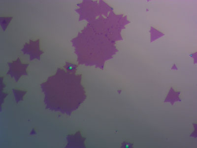
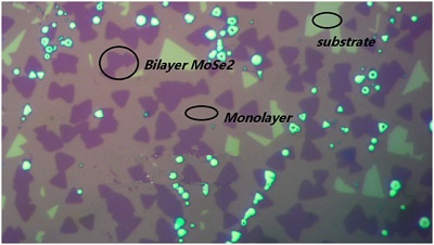
1) A single-layer discretely distributed triangular single crystal grain whose triangular side length is generally several tens micrometers.
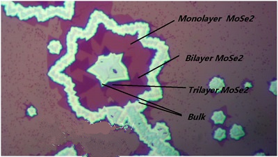
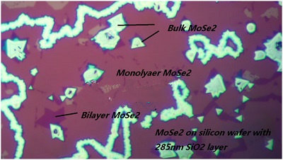
2) Continued growth from isolated grains A single layer of continuous film joined together with multiple layers on top.
3) Substrate: MoSe2 has many optional substrates, among which the most commonly used Si/SiO2 substrate are direct deposition products. Other substrates such as PET, PI, ITO, FTO, glass, metal substrates, etc. are transferred to the substrate desired by the customer after growth on sapphire.
Optoelectronic devices, microelectronic devices, biosensing, chemical sensing and other fields.
10 * 10mm, 15 * 15mm, 20 * 20mm, 2" disc, 4" disc or custom size specified by the customer.
Purification vacuum packaging, 1 piece / box, 5 pieces / box. 10 pieces / box.
Massachusetts Institute of Technology, California Institute of Technology, Stanford University;
Oxford University, Manchester University;
Seoul National University, Korea Institute of Science and Technology (KAIST), Sungkyunkwan University;Tokyo Institute of Technology, Murata Manufacturing Co., Ltd.,Tsinghua University, Peking University, Institute of Semiconductors, Chinese Academy of Sciences,And other world-class research institutions.

| Warm tip: the products supplied by Beijing Beike Xincai Technology Co., Ltd. are only used for scientific research, not for human body |
| Item ID | CAS | ID | Pack | Parameter | Stock | Make up | Price |
| BKTMDC123132-01 | BKTMDC123132 | 孤立晶粒 | 10mm*10mm | 100 | $865 | ||
| BKTMDC123132-02 | BKTMDC123132 | 连续薄膜 | 10mm*10mm | 100 | $865 |
|

| Reminder: Beijing Beike New Material Technology Co., Ltd. supplies products only for scientific research, not for humans |
| All rights reserved © 2019 beijing beike new material Technology Co., Ltd 京ICP备16054715-2号 |