Chemical Vapor Deposition, Chemical Vapor Deposition (CVD)
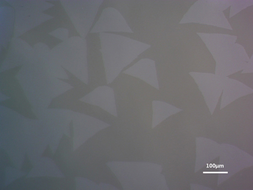
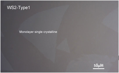
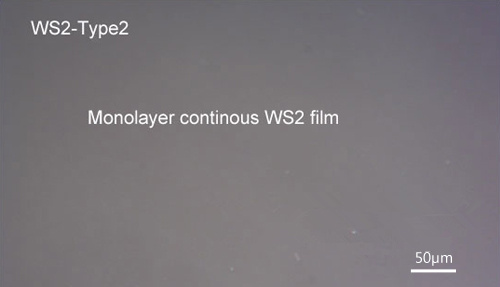
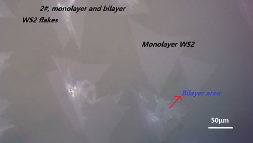
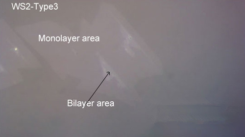
WS2 thin films are divided into various types:
1) Single-layer discretely distributed triangle-shaped single crystal grains, the triangle side length is generally tens to 100 microns.
2) The single-layer continuous film of Dalian continues to grow from triangular grains.
3) Multi-layer WS2 continuous film.
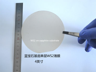
4) Substrate: WS2 has many optional substrates, among which the most commonly used sapphire substrates are direct deposition products. Other substrates such as PET, PI, ITO, FTO, glass, metal substrates, etc. are transferred to the substrates required by customers after growing on sapphire.
Optoelectronic devices, microelectronic devices, biological sensing, chemical sensing and other fields.
10*10mm, 15*15mm, 20*20mm, 2 inch wafer, 4 inch wafer or customized size specified by the customer.
Purified vacuum packaging, 1 piece/box, 5 pieces/box. 10 pieces/box.
MIT, Caltech, Stanford University;
the University of Oxford, University of Manchester;
Seoul National University, KAIST (KAIST), Sungkyunkwan University;
Tokyo Institute of Technology, Murata
, Tsinghua University, Peking University, Institute of Semiconductors
and other world-class research mechanism.
| Warm tip: the products supplied by Beijing Beike Xincai Technology Co., Ltd. are only used for scientific research, not for human body |
| Item ID | CAS | ID | Pack | Parameter | Stock | Make up | Price |
| BKTMDC123199-01 | BKTMDC123199 | 10*10mm | 100 | $588 |
|

| Reminder: Beijing Beike New Material Technology Co., Ltd. supplies products only for scientific research, not for humans |
| All rights reserved © 2019 beijing beike new material Technology Co., Ltd 京ICP备16054715-2号 |