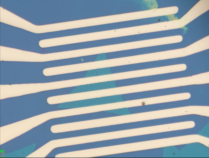
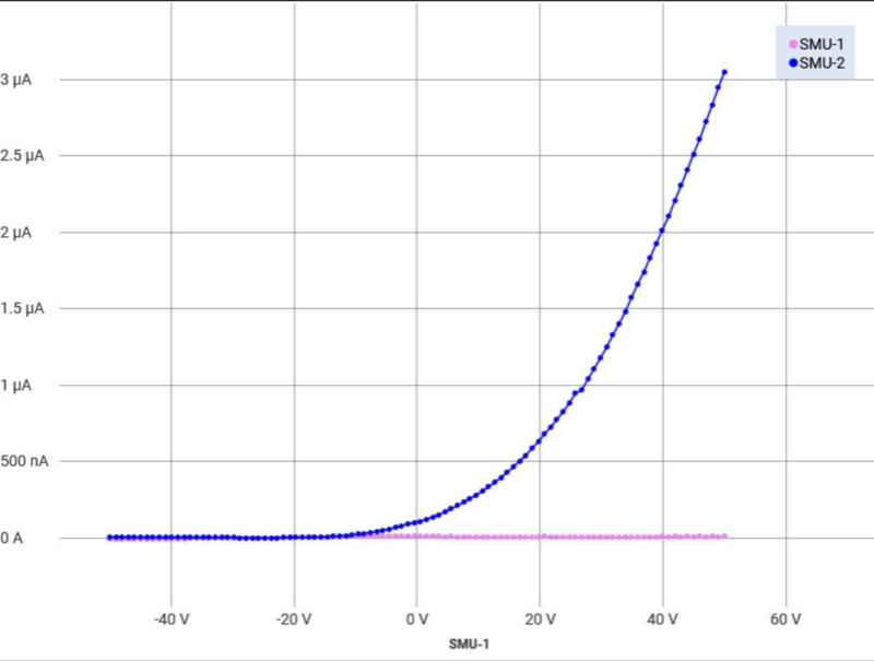
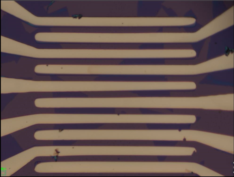
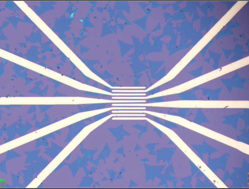
Device structure: conductive silicon wafer/300nm silicon oxide layer/triangular MoS2 or hand-tear single-layer MoS2/Au+Cr+Au electrode
Sample example
1) Mechanical lift-off of single-layer MoS2 back-gate FET (single-layer, 5um wide channel, 300nm silicon oxide substrate)
2) Mechanical lift-off few-layer MoS2 back-gate FET (~3 layers, 5um wide channel, 300nm silicon oxide substrate)
3) Mechanical lift-off of multilayer MoS2 back-gate FET (~5 layers, 5um wide channel, 300nm silicon oxide substrate)
4) CVD triangular MoS2 single crystal, back gate FET (single layer, 5um wide channel, 300nm silicon oxide wafer)
器件结构: 导电硅片/300nm 氧化硅层/三角MoS2 或者手撕单层MoS2/Au+Cr+Au电极


| Warm tip: the products supplied by Beijing Beike Xincai Technology Co., Ltd. are only used for scientific research, not for human body |
| Item ID | CAS | ID | Pack | Parameter | Stock | Make up | Price |
| BK2022062009 | BK2022062009 | 一片装 | 100 | $562 |
|

| Reminder: Beijing Beike New Material Technology Co., Ltd. supplies products only for scientific research, not for humans |
| All rights reserved © 2019 beijing beike new material Technology Co., Ltd 京ICP备16054715-2号 |