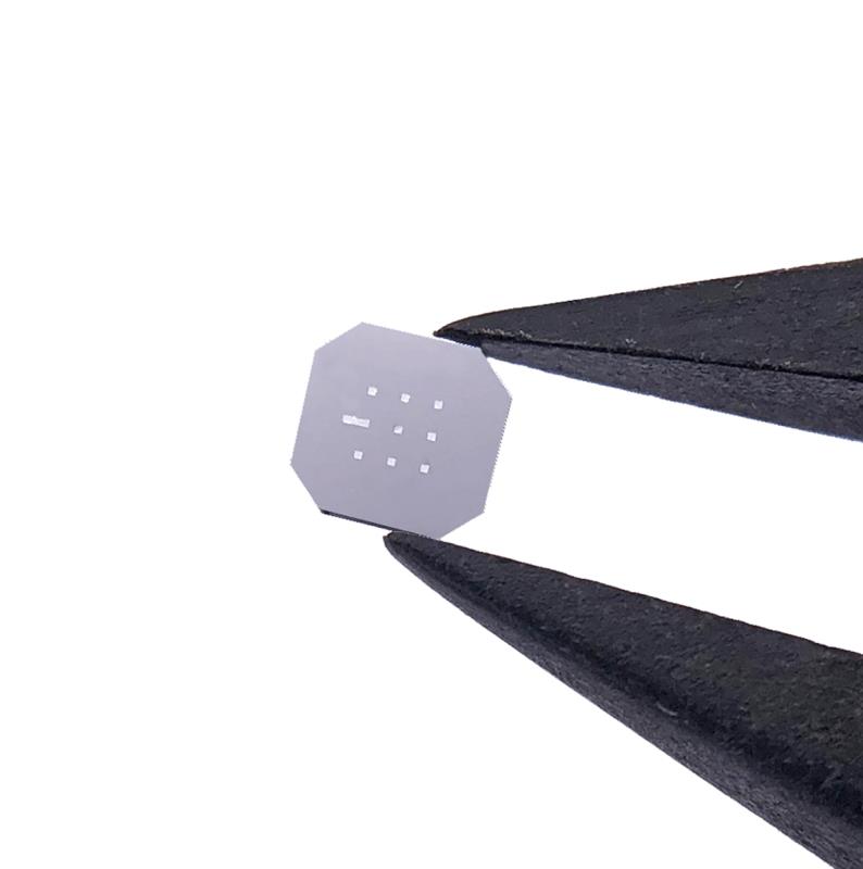
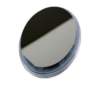
In order to meet the observation needs of scientific researchers on samples, we have adopted advanced microelectronics technology to design and manufacture standard silicon nitride film panes specifically for synchrotron radiation stations and scanning electron microscopes (SEM). Our silicon nitride film panes have the characteristics of high cleanliness, high X-ray transmission, low stress, high strength and uniform film thickness. They are suitable for high temperature (~ 1000 ℃) experiments and different pressure environments. At present, our products have been widely recognized by scientific researchers around the world and used in the research of biology, materials, physics, chemistry and other aspects.
Product features
Ultra clean
100-level clean environment
strictly selects silicon substrate materials.
Advanced process level
High strength
Thin film stress <250Mpa The
thinnest film can be up to 10nm
Window size can be up to 2cm
Ultra-flat
roughness less than 0.5nm
Uniformity is better than 5%
physical and chemical excelling
acid (excluding hydrofluoric acid), alkali resistance, organic solvent,
easy to clean using a plasma
X-ray transmission rate
Technical Parameters
|
Outer frame items
|
parameter
|
Outer frame items
|
parameter
|
|
material
|
N -type silicon
|
Resistivity
|
1 ~ 10 Ω-cm
|
|
Silicon nitride film parameters
|
parameter
|
Silicon nitride film parameters
|
parameter
|
|
material
|
LPCVD silicon nitride film
|
stress
|
<250MPa
|
|
Dielectric constant
|
6 -7
|
Dielectric strength
|
10 (10 6 V / cm)
|
|
Resistivity
|
10 16 Ω-cm
|
Roughness (Ra)
|
0.28 ± 5% nm
|
|
Refractive index @ 630nm
|
2.15-2.17
|
Roughness (Rms)
|
0.40 ± 5% nm
|
Application range

Nano materials, semiconductor materials, optical crystal materials, functional thin film materials

Characterization experiments of colloids, aerogels, organic materials and nanoparticles

Analysis of carbon-containing samples (photoresist, polymer, food, oil, fuel, etc.)

As a biological and cellular carrier
Product specification
This pane provides three different frame sizes (5mm, 7.5mm, 10mm) for selection. The thickness of the silicon substrate is 200μm.
|
Product ID
|
Film thickness
|
Window size
|
Frame size
|
|
|
TE025Z
|
10nm
|
0.25x0.25mm
|
5x5mm
|
|
|
TE050Z
|
10nm
|
0.5x0.5mm
|
5x5mm
|
|
|
TE025Y
|
20nm
|
0.25x0.25mm
|
5x5mm
|
|
|
TE050Y
|
20nm
|
0.5x0.5mm
|
5x5mm
|
|
|
TE025A
|
30nm
|
0.25x0.25mm
|
5x5mm
|
|
|
TE050A
|
30nm
|
0.5x0.5mm
|
5x5mm
|
|
|
TE100A
|
30nm
|
1x1mm
|
5x5mm
|
|
|
TE025B
|
50nm
|
0.25x0.25mm
|
5x5mm
|
|
|
TE050B
|
50nm
|
0.5x0.5mm
|
5x5mm
|
|
|
TE100B
|
50nm
|
1x1mm
|
5x5mm
|
|
|
TE150B
|
50nm
|
1.5x1.5mm
|
5x5mm
|
|
|
TE200B
|
50nm
|
2x2mm
|
5x5mm
|
|
|
TE025C
|
100nm
|
0.25x0.25mm
|
5x5mm
|
|
|
TE050C
|
100nm
|
0.5x0.5mm
|
5x5mm
|
|
|
TE100C
|
100nm
|
1x1mm
|
5x5mm
|
|
|
TE150C
|
100nm
|
1.5x1.5mm
|
5x5mm
|
|
|
TE200C
|
100nm
|
2x2mm
|
5x5mm
|
|
|
TE75050C
|
100nm
|
0.5x0.5mm
|
7.5x7.5mm
|
|
|
TE75200C
|
100nm
|
2x2mm
|
7.5x7.5mm
|
|
|
TE100300C (5pcs)
|
100nm
|
3x3mm
|
10x10mm
|
|
|
TE100500C (5pcs)
|
100nm
|
5x5mm
|
10x10mm
|
|
|
TE010D
|
200nm
|
0.1x0.1mm
|
5x5mm
|
|
|
TE025D
|
200nm
|
0.25x0.25mm
|
5x5mm
|
|
|
TE050D
|
200nm
|
0.5x0.5mm
|
5x5mm
|
|
|
TE100D
|
200nm
|
1x1mm
|
5x5mm
|
|
|
TE150D
|
200nm
|
1.5x1.5mm
|
5x5mm
|
|
|
TE200D
|
200nm
|
2x2mm
|
5x5mm
|
|
|
TE250D
|
200nm
|
2.5x2.5mm
|
5x5mm
|
|
|
Each box contains 10 chips (except some products)
|
|
Warm tip: the products supplied by Beijing Beike Xincai Technology Co., Ltd. are only used for scientific research, not for human body |
| Item ID |
CAS |
ID |
Pack |
Parameter |
Stock |
Make up |
Price |
| BK2020042701-21 |
|
BK2020042701 |
TE100300C(5pcs) |
3x3mm |
100 |
|
$0 |
| BK2020042701-22 |
|
BK2020042701 |
TE100500C(5pcs) |
5x5mm |
100 |
|
$0 |
| BK2020042701-23 |
|
BK2020042701 |
TE010D |
0.1x0.1mm |
100 |
|
$0 |
| BK2020042701-24 |
|
BK2020042701 |
TE025D |
0.25x0.25mm |
100 |
|
$0 |
| BK2020042701-25 |
|
BK2020042701 |
TE050D |
0.5x0.5mm |
100 |
|
$0 |
| BK2020042701-26 |
|
BK2020042701 |
TE100D |
1x1mm |
100 |
|
$0 |
| BK2020042701-27 |
|
BK2020042701 |
TE150D |
1.5x1.5mm |
100 |
|
$0 |
| BK2020042701-28 |
|
BK2020042701 |
TE200D |
2x2mm |
100 |
|
$0 |
| BK2020042701-29 |
|
BK2020042701 |
TE250D |
2.5x2.5mm |
100 |
|
$0 |